The entire signal chain accumulates and eventually affects the converter's error.
But keep in mind that the converter is the bottleneck of the signal chain and ultimately determines the accuracy of the signal representation. Therefore, the choice of converter is the key to setting the overall system requirements.
In the signal chain, there may be two types of errors that can accumulate - DC and AC errors.
DC or static errors (such as gain and offset errors) can help to understand the precision or sensitivity of the signal chain;
Communication-type errors, also known as noise and distortion, limit the system's performance and dynamic range.
Both types of errors need to be understood because both ultimately determine the resolution of the system. This article will specifically analyze DC errors and subdivide each inaccuracy based on its relationship with passive and active devices.
Before analyzing errors, first classify the signal chain
Figure 1 is a simple data acquisition system that can achieve 0.1% accuracy, that is, the output is either 0.99388V or 1.00612V for every 1V input. Therefore, the converter specifies a dynamic range of 60dB or 9.67ENOB, assuming a full-scale voltage of 10V. The converter has two amplifier stages, a multiplexer, and an ADC. This analysis will ignore sensors, cables, Connectors, PCB parasitic capacitance, and any external influences/errors, because these conditions are largely dependent on the specific application or signal we are measuring.

Figure 1. The design accuracy of this simple data acquisition signal chain system is 0.1%.
In order to provide reference for each error, the levels of analysis should be subdivided into parts. We divide the data acquisition signal chain into four levels -
The first level, a simple differential amplifier (Figure 2). The amplifier has a gain of 4× and an input impedance of 500 Ω. The capacitor is set for optional filtering.
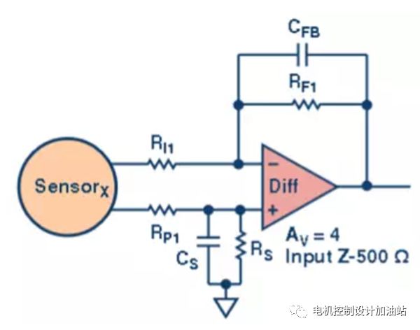
Figure 2. The differential amplifier is the first stage of the data acquisition signal chain.
In the second stage, the amplifier's output signal is applied to the multiplexer's eight inputs (Figure 3). Each input is buffered with a damping resistor (RO) to reduce charge kickback caused by multiplexer channel switching. According to the specification specified in the multiplexer data sheet, there is some parasitic capacitance or rated RO inside each channel.
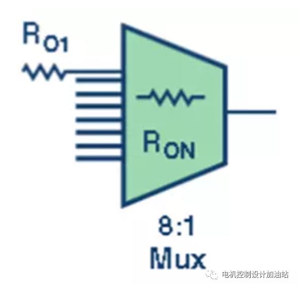
Figure 3. This 8:1 multiplexer has 8 buffered inputs.
In the third stage, the resulting channel signal is applied to the unity gain buffer stage amplifier (Figure 4). The resistor is used to reduce the input bias current imbalance.
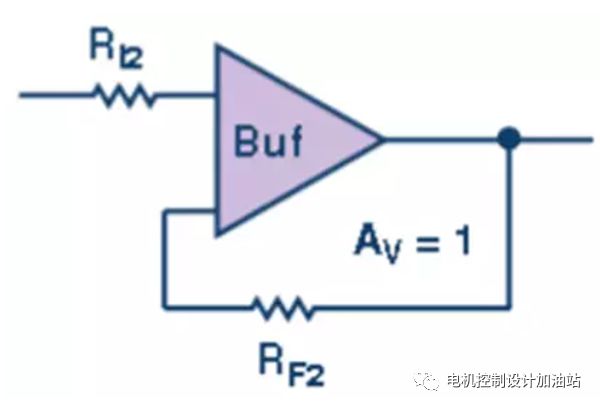
Figure 4. Apply a channel signal to this type of buffer amplifier.
In the fourth stage, the buffered signal is applied to a 12-bit, 1 MSPS ADC, where the signal eventually enters the digital domain (Figure 5). The serial resistor is used to buffer or suppress the signal between the amplifier and the converter, increasing the resistance between the two devices. As a result, the charge from the converter kickback to the amplifier is reduced, much like a multiplexer. This also helps to establish the output of the amplifier and prevent it from oscillating.
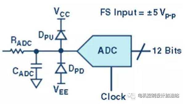
Figure 5. The signal buffer will be applied to a 12-bit, 1 MSPS ADC.
The capacitor provides a simple low-pass anti-aliasing filter (AAF) to attenuate signals and noise outside the target band. The design of the AAF depends to a large extent on the design and application of the system. Finally, the pull-up and pull-down diodes add input protection to prevent any fault conditions that could be caused by extreme overload signals that may be applied to the converter's input.
Next, we will examine passive and active errors based on the various signal chain stages discussed here.
DC passive error
All passive components have an error associated with it, especially the resistance. On the surface, the resistance seems to be a relatively simple device, but in fact, if its specifications do not meet the design requirements, it may cause errors in the entire signal chain. It will not discuss how to choose the correct type of resistor and its composition. But keep in mind that depending on the application, some resistance types may be more suitable than others.
Resistive DC errors result from unfavorable resistor tolerances. Simply specifying tolerance values ​​is not enough. However, overly discerning resistance error tolerances can also have an adverse effect, making the analysis too complex. When specifying the type of resistor for a given signal chain, at least four critical specifications must be observed:
Value tolerance, usually in %.
Temperature coefficient or drift in units of ppm/°C.
Life drift or eligibility, usually in % of a specified number of hours (usually 1000).
Value tolerance ratio, when there are two or more resistors in the network or in the same package and the values ​​match, the value tolerance is in %.
To illustrate how the resistance error accumulates (Figure 6), let's take a look at the following example: Assume a 100 Ω resistor with a tolerance of 1%, a temperature drift of 100 ppm/°C, and a tolerance for lifetime At 5%, the resistance is 93.15 Ω to 106.85 Ω over a temperature range of 85°C over a 5000-hour life cycle:

Figure 6. This figure shows a resistance error model.
Total tolerance (RVALUE + RTOL + RCOEFF + RLIFE) = (RVALUE + ((RTOL/100) × RVALUE) + (((RCOEFF × 0.000001) × temperature range) × RVALUE) + ((RLIFE/100) × RVALUE) ) = 94 Ω to 106 Ω.
Hard-won message edge note
Some components have a life cycle of only 1,000 hours, but the design requirements may be much longer, for example, 10,000 hours. To solve this problem, do not multiply 1000 hours by 8.77 (8766 hours/year); this is too pessimistic. Long-term drift in any precision analog circuit will have a certain amount of "random walk." The correct approach is to use the square root of this value, which is √ 8.766 = ~3 and then multiply by 1000 hours. Therefore, the 10,000-hour life cycle is: √ 10.000 = 3.16 × 1000 hours, and so on.
It should be noted that there are also errors in capacitance and inductance. However, these errors are usually negligible and there is not much value in such DC analysis. In addition, these devices are in fact reactive devices and have the greatest influence on filtering and bandwidth tolerance. This is not considered in the DC analysis of this paper.
DC active error
The signal chain described in Figure 1 uses the most common building block, which is a method of implementing a data acquisition system. The signal chain consists of two amplifiers, a multiplexer, and an ADC. But keep in mind that there are many types of active devices that describe various signal chains and different system topologies. When implementing this type of analysis, all active devices will have some type of dc error. In order to understand the accuracy of the system to be designed, it is important to decide which errors to consider.
Basically, two types/group errors are involved in DC accuracy. For all these active devices, these errors are both individual and universal. A single active device error will only show the known dc error relative to the device. This type of error can be found in the corresponding data sheet. For example, the input offset voltage of an amplifier can be considered as an individual error because this error is only the error specific to the active device.
The global error is the equal error that exists in each active device in the signal chain or system, but according to the different performance of the active device, it will show different errors (Figure 7). An example of a global error is the voltage regulation error of the bus supply and temperature. Next, we break down these errors for the three active devices shown in the signal chain one by one.
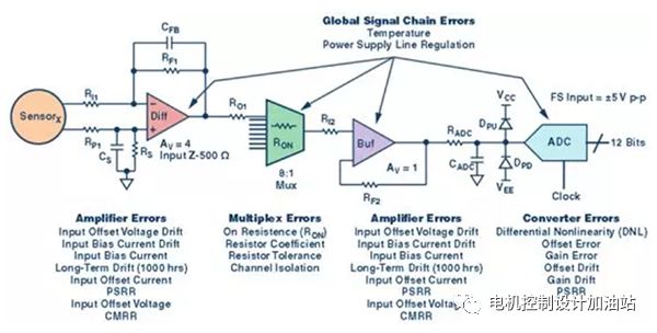
Figure 7. Active devices are affected by two types of dc precision errors - individual errors and global errors.
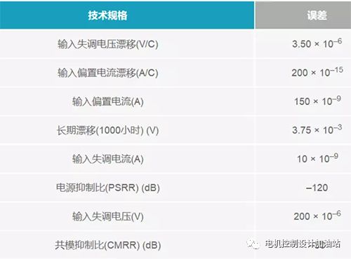
As we all know, the amplifier is still far from ideal. They have many errors and are generally listed in the data sheet. Offset voltage and bias current are two common errors, but any drift error, long-term error, and isolation error (such as power supply rejection ratio (PSRR)) must also be considered. Table 1 lists the following errors that should be considered when using the amplifier.
Table 1. Various errors of the amplifier
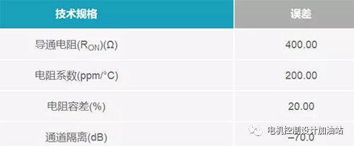
Multiplexers generally have less error than amplifiers. Among various multiplexer dc errors, on-resistance and channel isolation are the most influential errors. Table 2 lists the errors that should be considered when using multiplexers.
Table 2. Multiplexer errors
Offset, gain, and DNL are well-known and well-understood errors. Also include the PSRR. When using the ADC mentioned in the first section, the following converter errors should be considered:
The relative accuracy of DNL is defined as ±0.5 LSBs.
Relative accuracy temperature coefficient The DNL temperature coefficient is usually included in the data sheet's relative accuracy specification.
The gain temperature coefficient error is ±2.5 LSBs (data from the example above).
The offset temperature coefficient error is ±1.3 LSBs (data from the above example).
The power supply sensitivity is usually expressed in the low-frequency PSRR in the first Nyquist zone; for a 12-bit ADC, it is generally expressed as 60 dB or ±2 LSB.
To save space, we will not discuss in detail here how these errors are generated inside the active device. All of these errors are clearly defined and detailed in a large number of papers and articles. It should be noted here that all these basic errors must be taken into account to ensure that the analysis is reliable and that the system accuracy target specifications can be met.
In the above, the suggestions for the errors of individual active devices are given and their definitions are given. Next, the global errors should be considered. Such errors will affect the entire signal chain (Table 3). In this simple example, only the temperature and voltage regulation rate will be analyzed as a global error. However, it is also necessary to consider any other external influencing factors that are specific to the application or design.
Table 3. Global signal chain

Connect the device
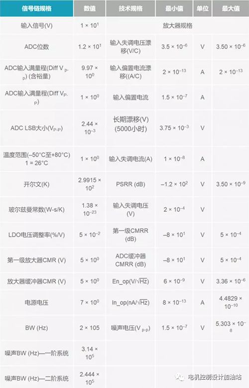
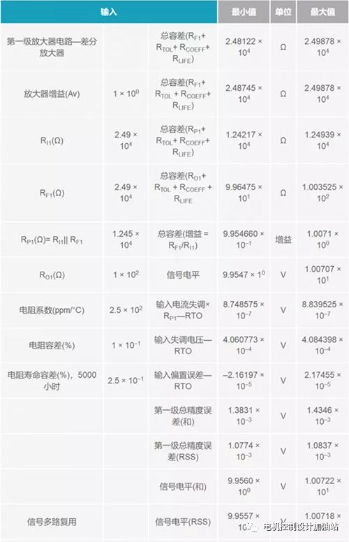
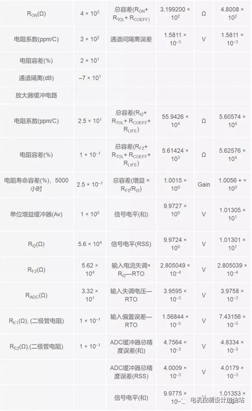
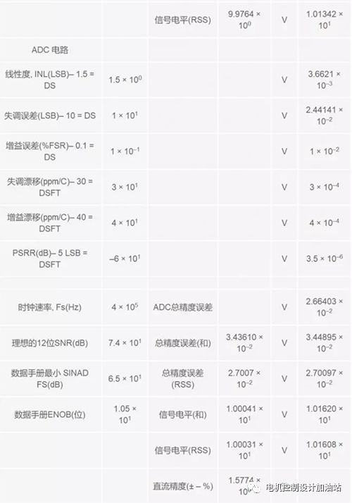
The foregoing defines all active and passive errors. Next, we must enter these errors into the spreadsheet to calculate the DC accuracy of the signal chain. Table 4 shows one way to accomplish this task.
Although there are many ways to analyze the precision of the signal chain, the spreadsheet method is the most flexible. This method also helps to understand how to subdivide all these error data in the signal chain design. With this approach, designers can quickly and effectively make trade-offs between the right devices for design considerations.
Take the time to compile an electronic form to make it layout reasonable and orderly. At the top of the table, global error and signal chain specifications are defined because these data affect the performance of the entire signal chain. Amplifier specifications/errors are also placed at the top because there are multiple errors and two amplifier stages in the entire signal chain.
Going down, on the left side of the table, subdivide all errors into each resistance level. The resistance error is also subdivided into levels to help understand the trade-offs. The right side shows the error of the read-through calculation and the cumulative calculation at each level of signal flow.
In the calculation results, all errors have been converted into voltage format. This is for convenience because the converter is at the end of the signal chain and its input full-scale is described with a voltage. RTO (Reference Output) is used to describe the successive accumulated errors from one level to the next. Each level also produces an independent total and RSS (and square root) total, to show how the error accumulates depending on the method used.
Therefore, based on the final results in Table 4, the cumulative total error is ±2.6% and the RSS error is ±1.6%. This is the error of the entire signal chain discussed in this article. The premise is the specification of the data sheet for each part and the above-mentioned global conditions at 26°C.
Table 4. Example of full-signal chain analysis
Cumulative total
Accuracy can be calculated in a variety of ways and it can take many forms. According to the designer's ideas, the methods used can be thoroughly understood and recorded to avoid erroneous results. Remember, in the first part, we mentioned that if you just use the root-sum-square (RSS) values ​​of all these error sources, the results may be too pessimistic. However, statistical tolerance results may be overly optimistic (sum of the total errors divided by the number of errors). The actual tolerance of the entire signal chain should be between these two ideas or methods.
Therefore, when adding (accumulating) accuracy errors throughout the signal chain, or when performing any system-accuracy analysis, designers should use the weighted error source method (as shown in the first part of the ADC example) and then perform these error sources. RSS calculations. This is the best way to determine the total error of the entire signal chain.
in conclusion
There are many kinds of errors in passive and active devices. Not all errors are important, but keep in mind those errors that are important for signal chain applications. Not all errors are valid for every application. When making any DC accuracy error analysis, it is an essential step to decide which of the most important or most influential or most weighted errors are.
Choosing the right passive device is as useful as the active device for the accumulated error in the signal chain. Preparing a spreadsheet and categorizing the data helps quickly consider a wide range of different devices and trade-offs. Finally, the accumulation of errors may appear in many different forms. The most common method is the RSS accuracy method.
However, one might think that the weighted sum error method is the correct way to determine the "worst-case dc error." Otherwise, this may easily lead to the design of the signal chain exceeding specification requirements, with more devices to compensate for the original set of errors. Not to mention the increase in costs and design factors such as size, weight, and power (SWaP).
Custom Wire Harness Assembly
- Electrified dimensional build boards with 100% continuity test
- Capabilities to test for fuse,diode,resistor, and relay presence
- Mating test fixtures for lower production wire harnesses
- Ability to free hand build harnesses for prototypes and design validation
- Separate layout boards for addition of fir tree clips, rosebuds, clamps,and labels after coverings added
- Capabilities to add board interlocks and test markings to harness as needed
Custom Wiring Harness,Wiring Harness,Cable Assemblies,Wire Harness,Wire Harness Assembly Manufacturer
ETOP WIREHARNESS LIMITED , https://www.oemwireharness.com