Frequency synthesizing technology has gone through three generations so far: direct frequency synthesis, phase-locked loop frequency synthesis, and direct digital frequency synthesis. Direct Digital Frequency Synthesis (DDFS or DDS) is a mark of the third generation of frequency synthesis technology. His main feature is that computers participate in frequency synthesis. They can be implemented either in software or in hardware. The combination of the two. The biggest advantage of the direct digital frequency synthesizer is that the frequency switching speed is extremely fast (up to a few microseconds), and the frequency, phase, and amplitude are all controllable. The output frequency stability can reach a stable metric level of the system clock, and it is easy to integrate. The main reason is that because computers participate in frequency synthesis, they can give full play to the role of software.
This article mainly introduces the realization of direct digital frequency synthesis based on single-chip microcomputer and CPLD.
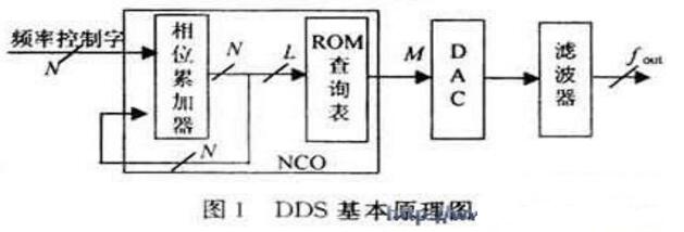
First, DDS worksThe block diagram of the DDS operation is shown in Figure 1. The essence of this is the sampling of the controllable interval between the reference frequency source (system clock) and the phase. As can be seen from FIG. 1, the DDS includes a numerically controlled oscillator (NCO), a DAC, and a low-pass filter (LPF), which are composed of a phase accumulator and a ROM look-up table. At each clock cycle, the N-bit phase accumulator accumulates its feedback value. The resulting high M bit is used as the address of the ROM lookup table and then read from the ROM to the DAC. The low-pass filter LPF is used to filter out higher harmonics in the DAC output. Therefore, the output frequency fout can be changed by changing the frequency control word K. The relationship between the output frequency fout and the frequency control word K is easily obtained: fout=Kfc/2N, where fc is the clock frequency of the phase accumulator and N is the number of bits of the phase accumulator. When K=1 is defined as the system frequency resolution, ie.
The system's functional block diagram is shown in Figure 2. This system is mainly composed of a single-chip microcomputer part, a DDS main channel part, a keyboard and a display part, and an output signal conditioning part.
Microcontroller chips use the more common AT80C31 chip. At the same time, it also extended a piece of program memory 2764 and data memory 6264, which are used to store the programs and random data needed during the operation.
The main part of the DDS is the key to our design. This part is mainly composed of the phase accumulation module, the address bus control module, the data bus control module and the waveform data memory EPROM, SRAM and so on. The phase accumulation module, the address bus control module, and the data bus control module are implemented on the CPLD. The chip used is the FLEX10K series of ALTERA devices. We solidified the required waveform sampling data in EPROM 2764, but we know that EPROM has a long read cycle and it is difficult to meet the access time requirements of the system. Therefore, one HSRAM is used in the design. In the course of the waveform synthesis in the DDS system, the waveform data can be quickly queried in place of the ROM.
The keyboard and the display section are important means for the system and the user to interact. This part of the logic function is also implemented on the CPLD.
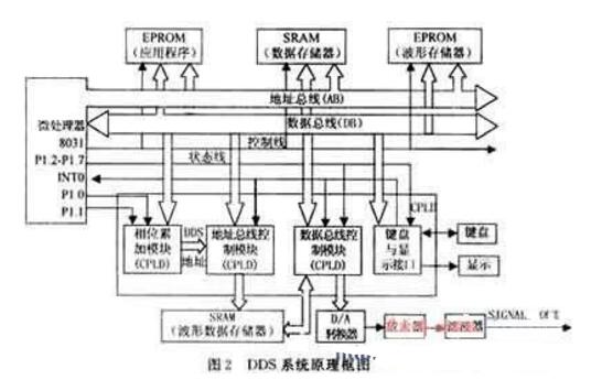
The output signal conditioning part converts the digital amplitude value of the waveform read from the HSRAM into an analog signal first, and then performs amplification and filtering to output. This section includes D/A converters, amplitude amplifiers, and filters. The DAC device uses AD's 12-bit AD9713B, which features a high update rate (100 MSPS) and low power consumption (725 mW), making it particularly suitable for DDS signal synthesis. The amplitude adjustment circuit uses a circuit consisting of the AD708, AD9617, and AD9713 bipolar amplifiers.
Third, the overall working status of the systemAs mentioned earlier, due to the relatively long read time of the EPROM, it is difficult to meet the system requirements for time. Therefore, a high-speed SRAM is added to the system as a waveform data buffer. In this way, the system has two working states: First, when the system starts working, the waveform data needs to be transferred from the EPROM to the HSRAM, that is, the loading state of the waveform data; after the data is loaded, the signal synthesis is performed according to the DDS synthesis principle, ie, the signal The synthesis state. The P1 port of the microcontroller is used in the system design to control the switching between these two operating states.
1, the loading of waveform data
After the power-on self-test of the SCM system is completed, the waveform data loading process begins. At this point, the address bus control module and the data bus control module hand off the control of the bus to the microcontroller system. In this process, the EPROM is in a read state and the SRAM is in a write state. According to the timing requirements of EPROM and SRAM, the 8031 ​​loads 8k waveform data from EPROM into HSRAM. This process takes about a few milliseconds.
From this we know that in this way not only can we synthesize standard waveforms (eg sine wave, square wave, triangle wave, etc.), but we can also synthesize various non-standard waveforms. In this case, we only need to obtain 8 K waveform data through a data collector or a PC, and then store it in the EPROM to output the corresponding waveform according to the required frequency.
2. Design of waveform synthesis circuit
After the waveform data is loaded, the system can perform signal synthesis. The single-chip microcomputer converts the received frequency value into a frequency control word and sends it to the phase accumulator. The phase accumulator accumulates the phase in every clock cycle, and then it will address the SRAM every time the sum is added as an address, read out the waveform amplitude value corresponding to the address, and send it to the D/A converter to convert it into an analog signal. Finally, the amplitude is amplified and filtered.
1) Reception and display of frequency values
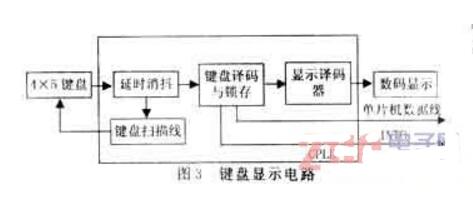
The keyboard and display section are used to implement the interaction between the user and the SCM. The system uses the interrupt query method to receive the frequency value input through the keyboard. The frequency value is sent to the digital display interface for display on the one hand, and converted into frequency control word to the phase accumulation module on the other hand. The keyboard display interface is shown in Figure 3. The dotted line in the figure is implemented by the CPLD.
2) Design and implementation of numerically controlled oscillator (NCO)
This part is a key part of DDS signal synthesis. It can be seen from the DDS system block diagram (Figure 2) that this part is mainly composed of a phase accumulator, an address bus controller, a data bus controller and an SRAM. Among them, in addition to SRAM, the remaining three modules are implemented on the CPLD.
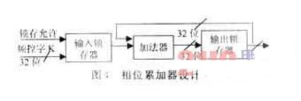
The phase accumulator is the key to the operation of the entire DDS system. Its design has a direct impact on the function of the entire system. As shown in Figure 4, it is essentially a 32-bit adder with feedback and performance. The output data is continuously added as the other input data and the frequency control word sent from the microprocessor to generate a regular 32-bit phase address code. The design uses pipeline technology to implement 32-bit adders. By inserting flip-flops between combinatorial logic, the transmission delay between registers is reduced, thus ensuring that the system can operate at higher clock speeds. 
The address bus control module and the data bus control module switch the system's address bus, data bus, and control line according to the different operating states of the system. The design of this part is relatively easy to implement and will not be described here.
3) Output signal conditioning section
This part consists of D/A converters, amplitude amplifiers, and filters. The circuit is shown in Figure 5.
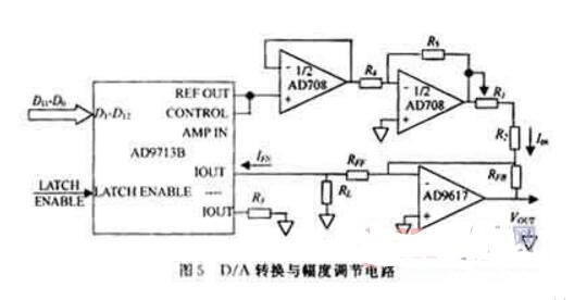
The DA device is selected from AD's high-speed chip 9713B, the chip's input is 12-bit. The amplitude adjustment circuit is composed of amplifiers. This is a current feedback high-speed amplifier circuit. It converts the current from the DA output to a voltage and determines the amplitude of the 9617 output by feeding back the current through the resistor RFB. RL and RFF act as a shunt to limit the current used for I/V conversion while providing an output voltage amplitude inside the 9617. The current flowing through R2 provides a DC bias to the 9617 output. Adjusting the value of R1 adjusts the bias current. The maximum amplitude of the entire amplifier circuit is ±4.096 V. The last part of the analog output is the filter circuit. The choice of filter depends on the waveform to be output by the system. For example, when we use DDS technology to synthesize sinusoidal signals, we can use elliptical filter.
IV. ConclusionCompared with the traditional frequency synthesis methods, the DDS synthesis method has a series of outstanding advantages such as fast frequency switching, high frequency resolution, and continuous phase change. Using the flexible control capability of the SCM and good man-machine conversational capabilities combined with the high performance and high integration of the CPLD, it can break through many design bottlenecks in the traditional design and greatly improve the performance of the system; at the same time, it is achieved in this way. The DDS circuit has great flexibility, and it can be designed according to the needs of the user to meet the special requirements of the user. Therefore, the system has a good development and application prospects.
At the same time, we should also pay attention to the inherent characteristics of DDS digitization, such as phase accumulator rounding, waveform amplitude quantization and non-ideal characteristics of DAC devices, making the output signal spectrum spurious. When the output frequency of the synthesized signal is relatively high, it is particularly prominent, thereby limiting the frequency range of the output signal. In this regard, on the one hand, we should minimize the various factors that can cause spurious in the design process, and more importantly, adopt technologies that facilitate CPLD implementation while effectively reducing output spurious, such as DDS phase accumulators. Improvements, ROM data compression, jitter injection techniques, etc. So that the developed DDS system performance is better.
The utility model relates to a medical atomization treatment and humidifying device belonging to the technical field of medical equipment and household appliances.
Professional Medical Atomization manufacturer is located in China, including Medical Vape,Dose Control Vape Pen,Supersonic Wave Vape, etc.
Medical Atomization,Medical Vape,Dose Control Vape Pen,Supersonic Wave Vape
Shenzhen MASON VAP Technology Co., Ltd. , https://www.disposablevapepenfactory.com