Abstract: This application note discusses the interface technology of 4.3Gsps downstream cable direct RF synthesis DAC MAX5881 and field programmable gate array (FPGA). The focus of the discussion is the timing of the interface between the MAX5881 high-speed digital input and Xilinx® Virtex ™ -5 FPGA. The techniques discussed here are equally applicable to many other FPGAs and custom ASICs.
Introduction Because the MAX5881 4.3Gsps downstream cable direct RF synthesis DAC has wideband characteristics, its data interface requires a higher operating frequency than narrowband DACs. Generally, when designing a broadband data interface, care must be taken to ensure that it works reliably and without errors.
Interface architecture FPGA functions can have many different combinations, there are several interface architectures to choose from, one of which is shown in Figure 1. This architecture can support a wider operating frequency range and has better tolerance for process, voltage, and temperature (PVT) changes. This application note focuses on the characteristics of this architecture. The specific timing analysis of the data interface highlights the advantages of this architecture compared to other architectures.
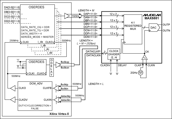
Figure 1. Interface between MAX5881 and Xilinx Virtex-5 FPGA (CLKDIV = 0, DDR data interface architecture)
Clock MAX5881 has independent analog and digital clocks. The MAX5881 provides clock output for digital data interfaces. Since the FPGA as the data source is not a data clock source, a "system synchronization" data interface¹ is required. It should be noted that the MAX5881 data clock output DATACLKP / DATACLKN jitter is very small, because it comes directly from the high-quality analog clock CLKP / CLKN input.
Use external clock feedback for FPGA DCM² to automatically compensate for the temperature-dependent output data clock inherent in FPGA Design the external clock feedback path so that it closely matches the delay of the MAX5881's DATACLKP / DATACLKN output to the FPGA internal data path. This ensures that the clock compensation provided by the Digital Clock Manager (DCM) is consistent with the FPGA clock and data path temperature drift. Make the PCB path of the clock feedback signal equal to the data path plus the DATACLK path length to ensure that the FPGA data output changes are consistent with the DATACLK edge. Adding additional delay to the clock feedback path can keep the data consistent with the clock. Design or adjust the delay to ensure the data stability of the MAX5881 from data establishment to hold time. The method of extending the length of the clock feedback signal path or adding an FPGA ODELAY device to the feedback path can be used to achieve this additional delay.
The data rate sets the MAX5881's CLKDIV pin to a low level, and the FPGA is configured for double rate (DDR) output data format. In this case, the frequency of the DATACLKP / DATACLKN signal is a quarter of the frequency of the clock input to the MAX5581 CLKP / CLKN pin. For the update rate of MAX5581, the frequency of CLKP / CLKN is 2.0GHz. Make the frequency of DATACLKP / DATACLKN 500MHz. This 500MHz clock signal is used to drive the FPGA serializer (OSERDES). The serializer is configured to output data on both the rising and falling edges of the clock. Therefore, the period of FPGA output data is 1ns (or 1.0GHz). Since Xilinx does not allow DCM (or PLL in this case) to be configured as external clock feedback and multiple output clocks, configuring CLKDIV = 0 can avoid generating a double frequency clock to drive the serializer. The OSERDES device at the data output stage at the end of the FPGA reduces the frequency of the upstream clock or OSERDES side data input. This makes FPGA placement and routing easy. For the update rate of the MAX5581, the frequency of the upstream clock is 250MHz.
Interface Timing Table 1 provides the timing analysis of the data interface in the form of a data table. The analysis is performed through two parts. The first part analyzes the working frequency of the interface, which is called "data cycle analysis". This section does not consider the exact location of stable data within the data period. However, it can determine whether it is possible to adjust the clock feedback delay to ensure the data stability of the MAX5881 from data establishment to data retention time window. The data table analyzes one operating frequency, and repeatedly analyzes several other operating frequencies (not shown). Figure 2 shows the analysis results. At the same time, Figure 3 shows the timing reference waveform.
Table 1. Data cycle analysis of the interface between Virtex-5 and MAX5881
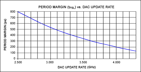
Figure 2. Period tolerance
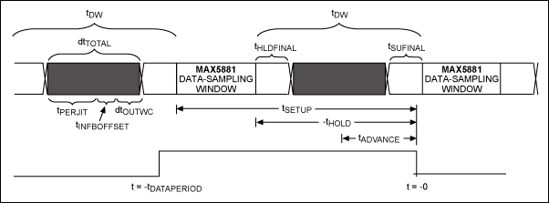
Figure 3. Timing reference waveform
The second part of the timing analysis calculates the required clock feedback delay (Table 2), and also calculates the setup and hold time tolerance corresponding to the feedback delay, or timing margin.
Table 2. Data timing analysis (MAX5881 pin DELAY = 0)
Similarly, this part of the analysis is repeated at various operating frequencies. Because the amount of data generated is too large, these data are not given in the table, but the graph is established using Figure 4 to establish tolerance and Figure 5 to maintain tolerance.
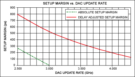
Figure 4. Establish tolerance
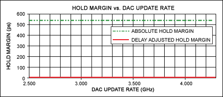
Figure 5. Maintain tolerance
It should be noted that in Figures 4 and 5, the clock feedback delay is calculated based on a wide operating frequency range (variable fDAC). The implementation method is to set the leading edge of the invalid data window, that is, at this position, the data begins to change to the next value after the MAX5881 hold time. In other words, once the hold time specification is met, the FPGA starts to switch to the next data value.
For a specific frequency, you can use the method of increasing the holding time tolerance and reducing the settling time tolerance to balance the settling time and holding time tolerance. This is achieved by inserting a variable delay in the clock feedback path. For low frequencies, the establishment and hold time tolerances are large enough, and the tolerance balance will be meaningless.
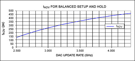
Figure 6. Tolerance balance
Other processing procedures due to the flexibility of FPGA devices, you can consider a variety of design methods. Studying the specific details of these methods is beyond the scope of this application note. Here are just a few of them:
Use the DCM phase offset to control the output data change, rather than increase the extra delay by increasing the length of the DCM clock feedback path. This method has advantages in software delay adjustment, but at the same time introduces more timing uncertainty brought by the FPGA phase shift circuit. Use ODELAY devices in the DCM feedback path. Similarly, it has advantages in terms of flexibility in software delay adjustment, but it also introduces more timing uncertainty. Use Method 1 or Method 2, but calibrate the devices one by one. The MAX5881 characteristic data shows that the change in the data sampling window of each device is 151ps compared to 340ps over the entire temperature range of all devices. Each device's small timing changes can compensate for FPGA timing uncertainty. Using this method, you can reduce some timing differences between FPGA devices. Conclusion By carefully selecting the system architecture, PCB design, and using specific designs, FPGAs can successfully interface with the MAX5881 and have positive data timing tolerance.
Introduction Because the MAX5881 4.3Gsps downstream cable direct RF synthesis DAC has wideband characteristics, its data interface requires a higher operating frequency than narrowband DACs. Generally, when designing a broadband data interface, care must be taken to ensure that it works reliably and without errors.
Interface architecture FPGA functions can have many different combinations, there are several interface architectures to choose from, one of which is shown in Figure 1. This architecture can support a wider operating frequency range and has better tolerance for process, voltage, and temperature (PVT) changes. This application note focuses on the characteristics of this architecture. The specific timing analysis of the data interface highlights the advantages of this architecture compared to other architectures.

Figure 1. Interface between MAX5881 and Xilinx Virtex-5 FPGA (CLKDIV = 0, DDR data interface architecture)
Clock MAX5881 has independent analog and digital clocks. The MAX5881 provides clock output for digital data interfaces. Since the FPGA as the data source is not a data clock source, a "system synchronization" data interface¹ is required. It should be noted that the MAX5881 data clock output DATACLKP / DATACLKN jitter is very small, because it comes directly from the high-quality analog clock CLKP / CLKN input.
Use external clock feedback for FPGA DCM² to automatically compensate for the temperature-dependent output data clock inherent in FPGA Design the external clock feedback path so that it closely matches the delay of the MAX5881's DATACLKP / DATACLKN output to the FPGA internal data path. This ensures that the clock compensation provided by the Digital Clock Manager (DCM) is consistent with the FPGA clock and data path temperature drift. Make the PCB path of the clock feedback signal equal to the data path plus the DATACLK path length to ensure that the FPGA data output changes are consistent with the DATACLK edge. Adding additional delay to the clock feedback path can keep the data consistent with the clock. Design or adjust the delay to ensure the data stability of the MAX5881 from data establishment to hold time. The method of extending the length of the clock feedback signal path or adding an FPGA ODELAY device to the feedback path can be used to achieve this additional delay.
The data rate sets the MAX5881's CLKDIV pin to a low level, and the FPGA is configured for double rate (DDR) output data format. In this case, the frequency of the DATACLKP / DATACLKN signal is a quarter of the frequency of the clock input to the MAX5581 CLKP / CLKN pin. For the update rate of MAX5581, the frequency of CLKP / CLKN is 2.0GHz. Make the frequency of DATACLKP / DATACLKN 500MHz. This 500MHz clock signal is used to drive the FPGA serializer (OSERDES). The serializer is configured to output data on both the rising and falling edges of the clock. Therefore, the period of FPGA output data is 1ns (or 1.0GHz). Since Xilinx does not allow DCM (or PLL in this case) to be configured as external clock feedback and multiple output clocks, configuring CLKDIV = 0 can avoid generating a double frequency clock to drive the serializer. The OSERDES device at the data output stage at the end of the FPGA reduces the frequency of the upstream clock or OSERDES side data input. This makes FPGA placement and routing easy. For the update rate of the MAX5581, the frequency of the upstream clock is 250MHz.
Interface Timing Table 1 provides the timing analysis of the data interface in the form of a data table. The analysis is performed through two parts. The first part analyzes the working frequency of the interface, which is called "data cycle analysis". This section does not consider the exact location of stable data within the data period. However, it can determine whether it is possible to adjust the clock feedback delay to ensure the data stability of the MAX5881 from data establishment to data retention time window. The data table analyzes one operating frequency, and repeatedly analyzes several other operating frequencies (not shown). Figure 2 shows the analysis results. At the same time, Figure 3 shows the timing reference waveform.
Table 1. Data cycle analysis of the interface between Virtex-5 and MAX5881
| Value | Unit | SpecificaTIon | DescripTIon | Source | Notes |
| 4.300 | GHz | fDAC | MAX5881 output update rate | MAX5881 data sheet | |
| 0.5375 | GHz | fDATACLK = fDAC / 8 | DDR interface mode | MAX5881 data sheet | |
| 930 | ps | tDATAPERIOD = 1 / (2 × fDATACLK) | Data period | MAX5881 data sheet | |
| 50 | ps | TINFBOFFSET | FPGA DCM feedback phase error (peak ±) | Xilinx ds202.pdf | |
| 120 | ps | tPERJITT | FPGA DCM jitter (peak ±) | Xilinx ds202.pdf | |
| 121 | ps | dtOUTWC | Worst PVT FPGA output-to-output skew (peak-to-peak) | ".twr" post-layout staTIc timing report from Xilinx static timing analyzer (worst-case PVT) | |
| 1.4 | ps | dtPCB | Board output-to-output skew | Estimate | All PCB data and data clock trace lengths matched |
| 462 | ps | dtTOTAL = (2 × tINFBOFFSET) + (2 × tPERJITT) + dtOUTWC + dtPCB | Total FPGA data output timing variance | ||
| 1100 | ps | tSETUP | MAX5881 setup time | MAX5881 data sheet | |
| -760 | ps | tHOLD | MAX5881 hold time | MAX5881 data sheet | |
| 590 | ps | tDW = tDATAPERIOD-(tSETUP + tHOLD) | MAX5881 data change window | Time in clock period when data does not have to be valid and stable | |
| 128 | ps | tPSL = tDW-dtTOTAL | Period timing slack | Extra time between FPGA changing data; data must be stable at DAC |

Figure 2. Period tolerance

Figure 3. Timing reference waveform
The second part of the timing analysis calculates the required clock feedback delay (Table 2), and also calculates the setup and hold time tolerance corresponding to the feedback delay, or timing margin.
Table 2. Data timing analysis (MAX5881 pin DELAY = 0)
| Value | Unit | Specification | Description | Source | Notes |
| 0 | ps | tDOUTNOM | FPGA clock-to-data output delay | FPGA external clock-feedback configuration | Feedback-path length equal to data-path length plus clock-path length; this centers data transitions at the clock edge |
| -170 | ps | tSUNOM = tDATAPERIOD-tSETUP-tDOUTNOM | Nominal setup margin (without dtTOTAL factor) | Calculate margin without jitter, skew, and phase-error effects first; they are accounted for later | |
| 760 | ps | tHLDNOM = tDOUTNOM-tHOLD | Nominal hold margin | Calculate margin without jitter, skew, and phase-error effects first; they are accounted for later | |
| -401 | ps | tSUABS = tSUNOM-dtTOTAL / 2 | Absolute setup margin (including dtTOTAL factor) | Include jitter, skew, and phase-error effects | |
| 529 | ps | tHLDABS = tHLDNOM-dtTOTAL / 2 | Absolute hold margin (including dtTOTAL factor) | Include jitter, skew, and phase-error effects | |
| -529 | ps | tDADVANCE = -tHLDABS | Delay-adjusted FPGA clock-to-data output | External clock feedback with feedback-path length equal to data-path length plus clock-path length plus tHLDABS | Place data transition immediately after tHOLD |
| 128 | ps | tSUFINAL = tSUABS-tDADVANCE | Delay-adjusted setup margin | ||
| 0 | ps | tHLDFINAL = tHLDABS + tDADVANCE | Delay-adjusted hold margin |
Similarly, this part of the analysis is repeated at various operating frequencies. Because the amount of data generated is too large, these data are not given in the table, but the graph is established using Figure 4 to establish tolerance and Figure 5 to maintain tolerance.

Figure 4. Establish tolerance

Figure 5. Maintain tolerance
It should be noted that in Figures 4 and 5, the clock feedback delay is calculated based on a wide operating frequency range (variable fDAC). The implementation method is to set the leading edge of the invalid data window, that is, at this position, the data begins to change to the next value after the MAX5881 hold time. In other words, once the hold time specification is met, the FPGA starts to switch to the next data value.
For a specific frequency, you can use the method of increasing the holding time tolerance and reducing the settling time tolerance to balance the settling time and holding time tolerance. This is achieved by inserting a variable delay in the clock feedback path. For low frequencies, the establishment and hold time tolerances are large enough, and the tolerance balance will be meaningless.

Figure 6. Tolerance balance
Other processing procedures due to the flexibility of FPGA devices, you can consider a variety of design methods. Studying the specific details of these methods is beyond the scope of this application note. Here are just a few of them:
Use the DCM phase offset to control the output data change, rather than increase the extra delay by increasing the length of the DCM clock feedback path. This method has advantages in software delay adjustment, but at the same time introduces more timing uncertainty brought by the FPGA phase shift circuit. Use ODELAY devices in the DCM feedback path. Similarly, it has advantages in terms of flexibility in software delay adjustment, but it also introduces more timing uncertainty. Use Method 1 or Method 2, but calibrate the devices one by one. The MAX5881 characteristic data shows that the change in the data sampling window of each device is 151ps compared to 340ps over the entire temperature range of all devices. Each device's small timing changes can compensate for FPGA timing uncertainty. Using this method, you can reduce some timing differences between FPGA devices. Conclusion By carefully selecting the system architecture, PCB design, and using specific designs, FPGAs can successfully interface with the MAX5881 and have positive data timing tolerance.
3.2V105Ah Lithium Ion Battery,105Ah 3.2V Phosphate Battery Cell,3.2V105Ah Deep Cycle Solar Battery,3.2V 105Ah Lifepo4 Forklift Battery
Jiangsu Zhitai New Energy Technology Co.,Ltd , https://www.ztbatteries.com