Hi everyone, I’m Haikun Jia, and I’m very happy to have this opportunity to share some experience in electromagnetic field simulation with you. Let me briefly introduce myself. I graduated with a bachelor’s degree in 2009 and a Ph.D. in 2015. I followed Professor Wang Zhihua on the design of millimeter-wave integrated circuits. I usually write some technical articles on circuit design and post them on my personal public account and Zhihu column. Friends who are interested can pay attention to them. This time the text of the lecture will also be posted after it has been sorted out.
Today I mainly want to share with you the practical experience of electromagnetic field simulation and millimeter wave chip design. These are some thoughts and summaries of my usual design. I hope to inspire you.
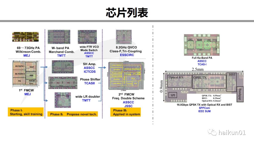
This picture shows the chips designed during my Ph.D. and postdoctoral period. Most of them are millimeter wave circuits, with modules and systems. In the past four or five years, there is a deep feeling in the process: that is, as more and more circuits are made, my understanding of millimeter wave circuit design has been deepening.
Give two examples. One is that we almost only use transmission lines for the first version of the chip. Why? Because the transmission line is simple, the simulation is not easy to make mistakes, and the design iteration is also simple. But the actual design is greatly restricted. Later, with some experience, I started to use inductors. Later, a large number of transformers began to be used. The second example is a transformer. When I first used a transformer, the transformer was like a black box to me, probably imitating a transformer, and an additional transmission line was added outside for matching. This is not impossible. But not good enough. Later, I began to understand the internal characteristics of the transformer, it has inductance and coupling. Later, it was discovered that considering inductance and coupling was not enough, and parasitic capacitance had to be added. If we look at the on-chip transformer today, it has multiple parameters, each of which has its own role, and each parameter should be optimized. When designing, I must first know what kind of transformer I need, and then the electromagnetic field tool is an auxiliary means to help me find the transformer I want.
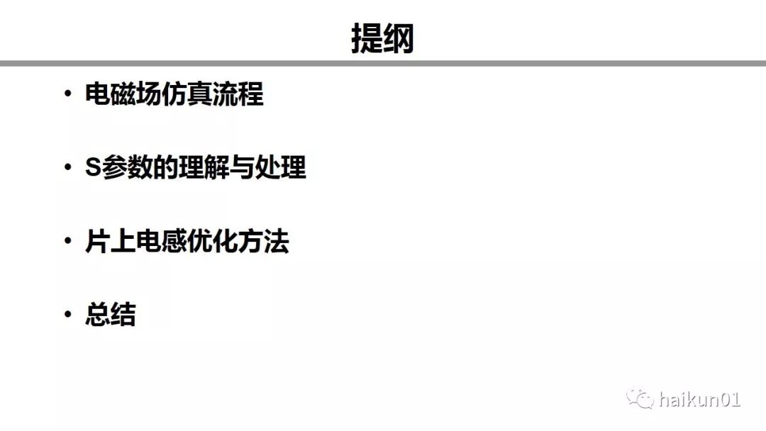
This is the main content of this sharing, the electromagnetic field simulation process, the understanding and processing of S parameters, the optimization of on-chip inductance, and the final summary.
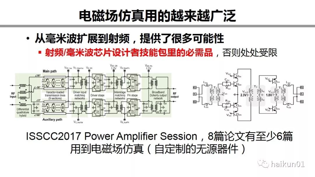
In recent years, it has been discovered that electromagnetic field simulation has become more and more widely used. It is definitely not only used in the millimeter wave frequency band, but also a large number of electromagnetic field tools are used in the radio frequency band. For example, in the 2017 ISSCC power amplifier, at least 6 of the 8 papers need to use electromagnetic field simulation tools. These are two of the circuits. It can be seen that a large number of transformers and transmission lines are used. As far as I know, the foundry does not provide a model of the transformer. If you don't know how to use electromagnetic field simulation, then the transformer cannot be used. Therefore, electromagnetic field simulation is an essential skill package for RF millimeter wave chip designers, otherwise it will be restricted everywhere.
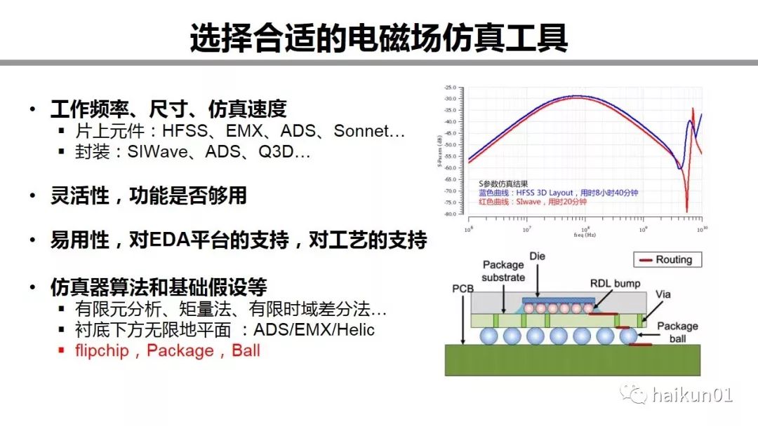
Choosing a suitable electromagnetic field simulation tool can mainly be considered from these aspects.
The first one is the frequency and size of the passive structure we want to imitate. If there are on-chip components, HFSS, EMX, ADS, Sonnet, Helic are all good choices. For packaging and PCB, you may choose SIWave, ADS, Q3D, etc. I used to compare my SIwave and HFSS 3D Layout simulation for the same high-speed package, and got similar results, one took 20 minutes and the other was 9 hours faster.
The second is flexibility, whether the function can meet the demand.
The third, ease of use, support for the EDA platform. There is also support for craftsmanship. In the past, we used the 65nm process, which was a tech file based on the document. It is estimated that the current advanced technology will not work. One is that many key information of the foundry is encrypted, and the other is that it has some layout dependent parameters. For example, if you spend a 1um thread, the final product may not be 1um, and the foundry will make some adjustments. Now it is usually which electromagnetic field software you bought. He has contacted the foundry and has written the tech files, all of which are taken into account.
The fourth is the simulation principle used by the software. The principle part will not be elaborated. If you are interested, you can read an article on my official account. The assumption behind the simulator is very important. Like EMX and Helic, they can only simulate layered structures and assume an infinite ideal ground plane when the substrate is on the ground. This is generally not a problem, but if your substrate is very thin, It may be wrong to imitate it.
Many chips are now flip-packaged, so there will be a layer of metal on top of the chip. If EMX and HELIC are used for simulation, this is not taken into consideration. I used HFSS to build a model and tried it once. If the distance is less than 50um, the inductance will be affected by about 10%. I asked about the technical support of the software we used, and he said that some customers would indeed verify the impact of the package. This requires manual modification of the tech file and adding a metal layer on the chip, which would be more troublesome in actual operation.
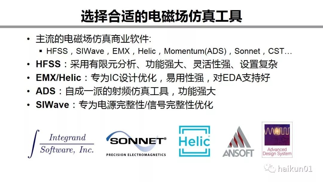
There are actually many mainstream electromagnetic field simulation tools. It is estimated that the first three are more popular. The HFSS function is the most flexible and powerful. In theory, any structure can be imitated, but the support for the EDA platform is general. It is used more in schools. EMX/HELIC is specially optimized for IC design and has better ease of use.
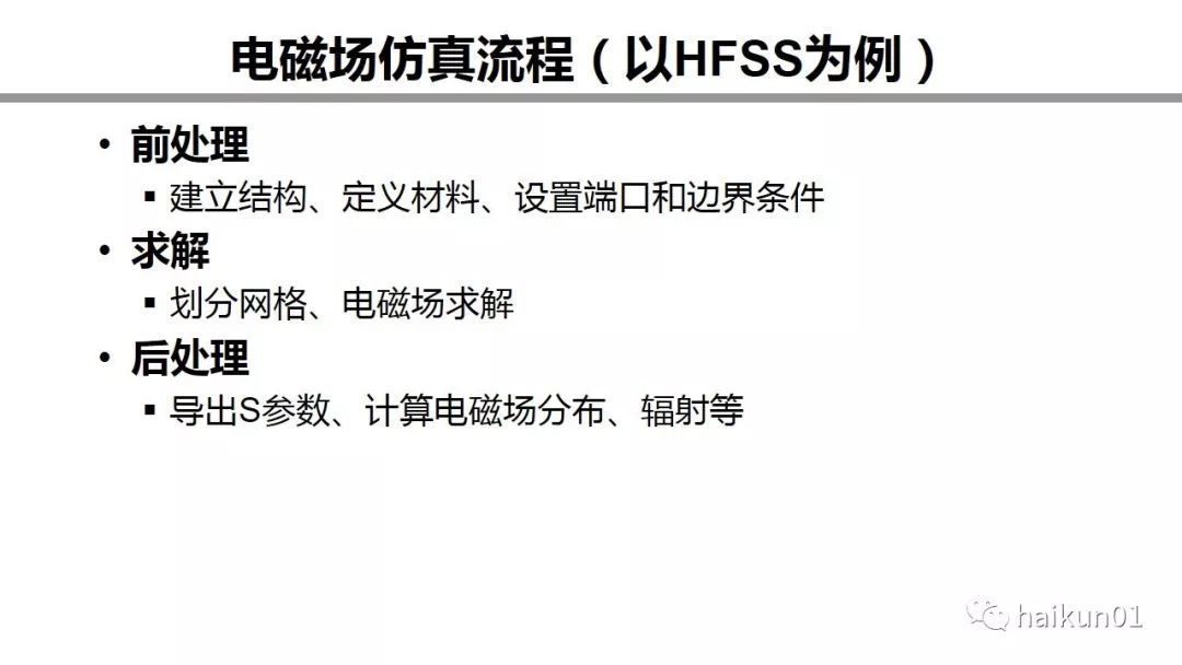
Okay, let's talk about the electromagnetic field simulation process, here we mainly take HFSS as an example. The EMX process is simpler, and the software has already been considered for designers in many places.
The solution process of almost any electromagnetic field simulation software is these three steps. The first is pre-processing, including building structure, defining materials, setting ports and boundary conditions, etc. The second is to divide the material into fine grids, and then solve the differential equation or integral equation of the electromagnetic field to solve the field strength everywhere. But our circuit designers cannot directly use the field strength in circuit design, so post-processing is needed. Post-processing includes deriving S parameters, calculating electromagnetic field distribution, radiation, and so on.
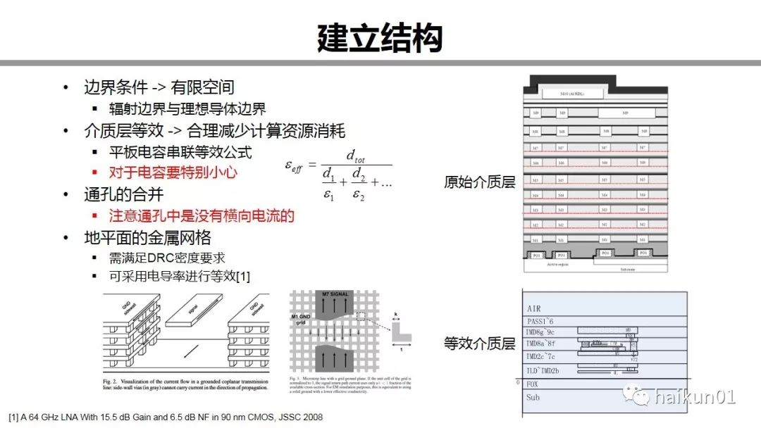
Now let's see how to build the structure. The first is the boundary conditions. We can only simulate the content of a limited space, so we generally set the radiation boundary for the air box and the ideal conductor boundary for the bottom surface of the substrate. The second is the equivalent of the medium layer, which can reasonably reduce the consumption of computing resources. Pay special attention to the capacitance here, because it is easy to change the capacitance value when the dielectric layer is equivalent. The upper picture on the right is the original dielectric layer, and the picture below is after the equivalent. You can see that the middle layer of the MIM capacitor is not equivalent to me. For through holes, we usually merge, and this step is done in the layout. But note that there is no lateral current in the through hole. If you run the lateral current in the through hole after the equivalent, the result will be a little different. The last is the ground plane. In order to meet the DRC rules, we will hollow out the ground plane. These holes will cause the simulation to be slower, so it can be equivalent to the entire flat plate, reducing the conductivity appropriately.
In EMX, these softwares have already been done for help, so there is no need to think about it.
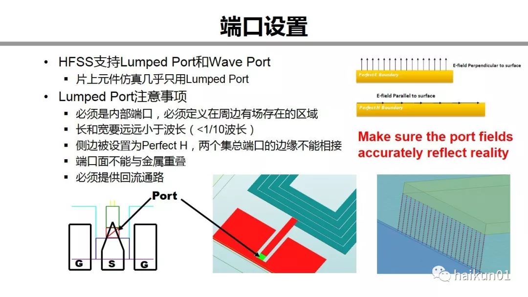
Now look at the port settings. This step is especially important. Whether the result of electromagnetic field simulation is reasonable depends largely on whether the port setting is reasonable. There are two types of ports in HFSS, centralized port and wave port. But we almost only use centralized ports. What kind of incentives does the centralized port provide? It can be seen from this figure that it is an electric field uniformly distributed across the entire surface from the upper edge to the lower edge. When setting up any port, we need to think about whether the actual field strength will really be distributed like this. So this one is easy to understand. If there is a very long port, the simulator will assume that the electric field of the whole port is uniform, but in fact it will show a certain distribution, which does not match the actual situation, and the calculation result is wrong. EMX and ADS also have this problem. If you want to add incentives on the long side, they both suggest to draw a short side on the long side and add the excitation on the short side.
I used HFSS to imitate an inductor, and the result was very strange. Later, when I checked it, I found that the concentrated port surface overlapped with the metal, so he forced him to think that there was also a uniform field in the metal cross section. The imitation result was definitely not correct.
The last one is that HFSS needs to consider EMX without too much consideration, that is, HFSS must provide a return path for the centralized port. Therefore, our imitation inductors generally add a circle of ground plane outside.
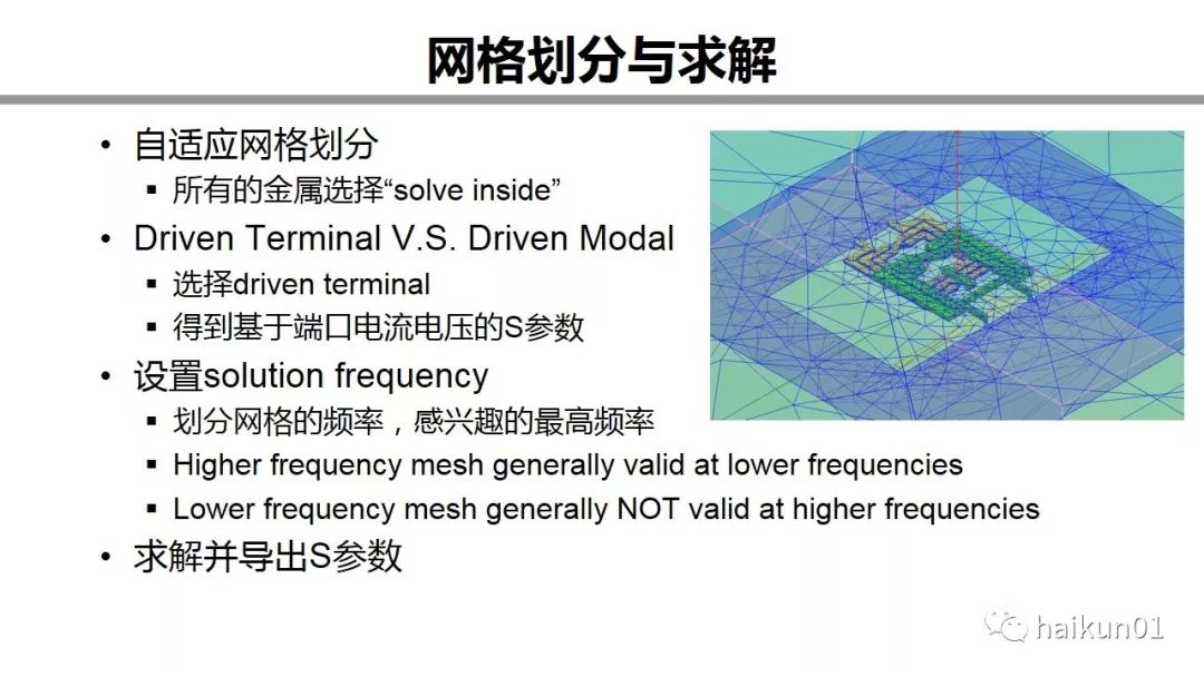
There is not much attention to meshing and solving. First, choose solve inside for all metals, otherwise the Q value will be inaccurate. It is not selected by default. Second, choose the solution method of Driven terminal. Third, the solution frequency, that is, the frequency of the division of the grid, tends to set this frequency a little higher, so that the division of the grid is detailed and the result is more accurate. In this way, S parameters can be derived after imitating.
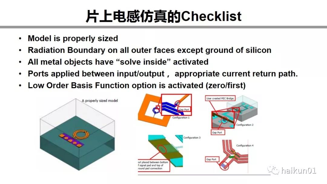
Here is a summary of the Check list of HFSS inductance simulation. You can develop a habit of checking it every time you finish setting it. The model size is appropriate, the radiation boundary and the ideal conductor boundary, all metals have a solve inside, the port has a return path, and a low-order basis function is selected. The addition of common inductance simulation ports is drawn here.
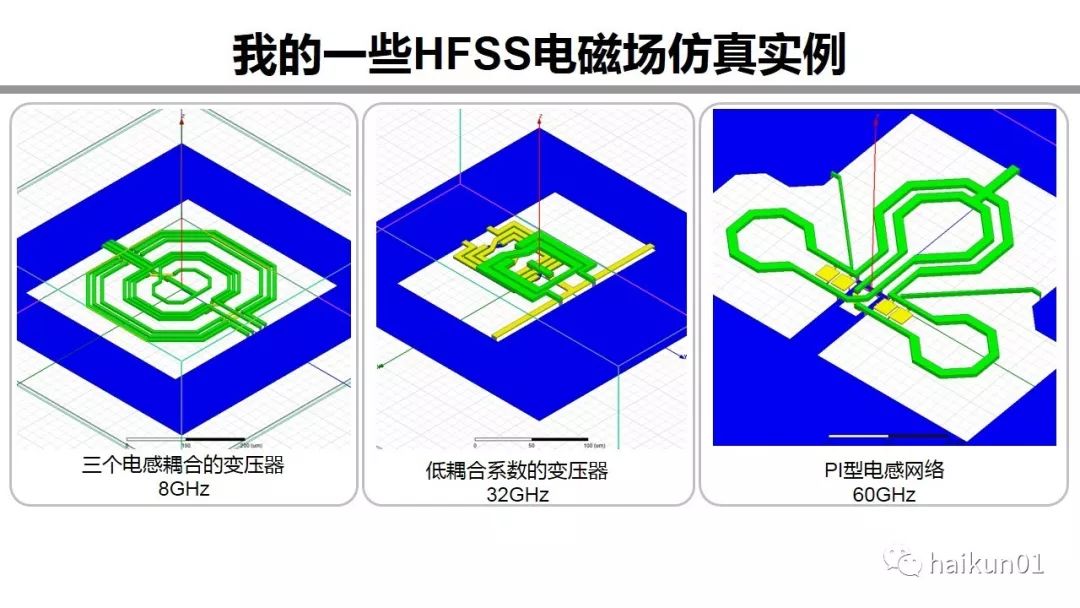
This picture shows the structure of some passive devices that I have imitated before. Both the substrate and the air box are transparent, so they cannot be seen. The blue metal is the ground plane, which is used to provide a return path. These three frequencies gradually increase. An interesting rule is that the lower the frequency, the more complex the structure can be.
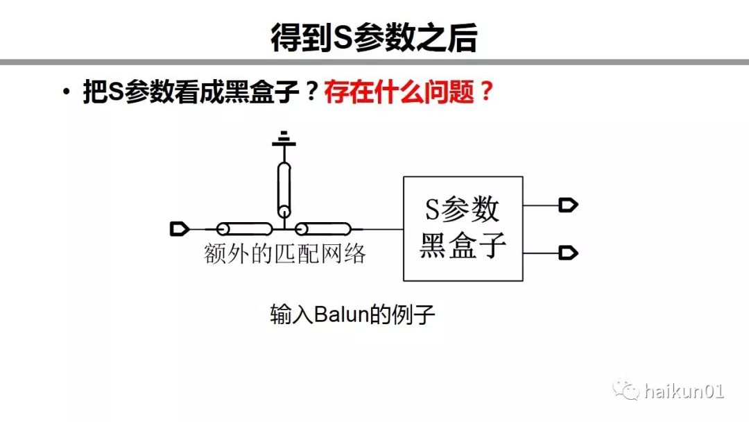
If we now get the S-parameters, can we use the S-parameters in the simulation? How to use it? One way is to treat S-parameters as a black box. I did this in the first place. I need a single slip Balun, so I roughly imitated a transformer, and then found that the input did not match, and added three additional transmission lines for input matching. This is not impossible to design. But what's the problem? First, additional matching consumes additional area and increases loss. Second, if you don't understand the internal structure of the S-parameters, you will be less confident. Third, you can't do theoretical analysis, and you can't write a thesis. Fourth, treating the S parameter as a black box gives up a lot of possibilities. Originally, the transformer can be used for broadband matching, but the black box cannot be optimized for you. You have a good idea, but it is very likely that it is not optimized here and not optimized there. In the end, the good performance of your idea will be completely offset by these areas.
So we said that after you get an S parameter, you don't just throw it into the emulator. You also need to understand the S parameter.
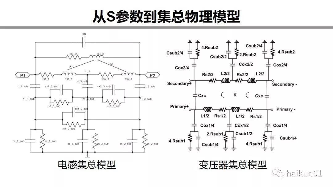
How to understand it? The first method is to transform it into a lumped model. Here are examples of the inductance lumped model and the transformer lumped model.
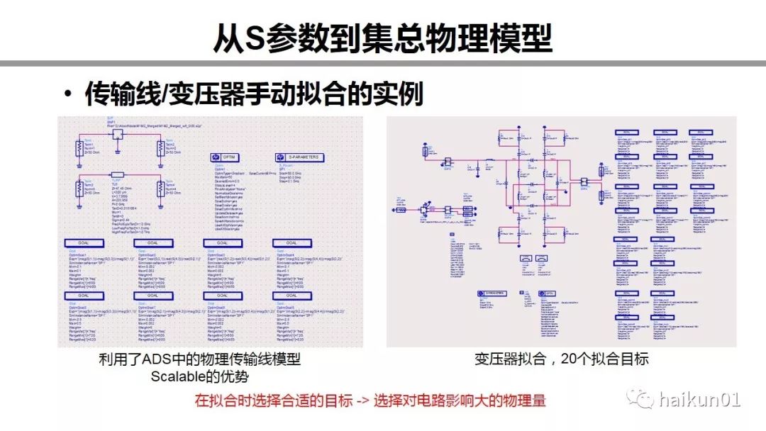
For HFSS users, this step of conversion has to be done by yourself. These are two fitting examples. The principle is very simple. You simultaneously imitate the S parameters and your model, set some goals, and let the simulator optimize the parameters to achieve the goal. For the simulation of the transmission line, the physical transmission line model in ADS can be used, which is very useful. After fitting, you can freely change the length of the transmission line, which is equivalent to a scalable model. The picture on the right is the fitting of the transformer. Here I used 20 targets.
The selection of the fitting target requires some consideration. For example, two-port S-parameters, the real part and the imaginary part have a total of 8 parameters. You can use S-parameter fitting or Y-parameter fitting. But I think we should choose the physical quantity that has a great influence on the circuit to fit. For example, if we want to fit the input match, I can use the amplitude to fit, or I can take dB and then fit. But the amplitude is obviously better. The return loss of -30dB and -40dB has no effect on the circuit, but there is a 30% difference in value. The operation of taking dB is equivalent to amplifying the weight of the small signal part.
EMX provides some preset model fittings. But there are also great limitations. If two or three devices are together, he can't fit them.
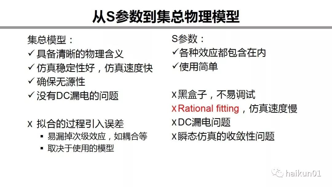
Both S-parameter simulation and physical lumped model simulation have their own advantages. The centralized model simulation has good stability and fast speed. Passive performance is guaranteed. There is no leakage problem. However, there is a point that needs to be paid attention to when using physical lumped model to simulate. When we are fitting, we actually lose some high-order effects, such as the weak coupling between two inductors. Generally no problem, but on some occasions it can have a serious impact. For example, for two clocks with different frequencies, the clock signal may be coupled through passive components to cause crosstalk, and directly converted to Jitter, which requires high isolation, and weak coupling also has an impact. If a centralized model is used, it is difficult to fit such a weak coupling.
So in the end, everyone will use S-parameters to imitate a whole, including all kinds of effects. But S-parameter simulation often encounters some headaches. There are some recommended settings and solutions. I won't talk about it here.
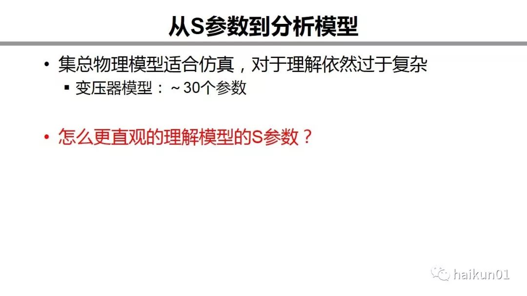
Okay, now we have the lumped model, but it is still too complicated for understanding. The previous transformer has 30 parameters, which I cannot take into account in the theoretical calculations. Then how do we understand the S parameters of the model more intuitively?
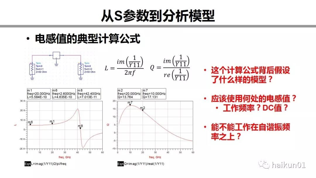
I take inductors as an example here. If we get the S parameter of an inductor, we know that we can use these two formulas to calculate the inductance value and the Q value. The typical curve obtained looks like this. Now here comes the problem. What model is assumed behind this calculation formula? This inductance value changes with frequency, so what frequency should we use? Operating frequency or DC frequency? Can this inductor work above the self-resonant frequency?
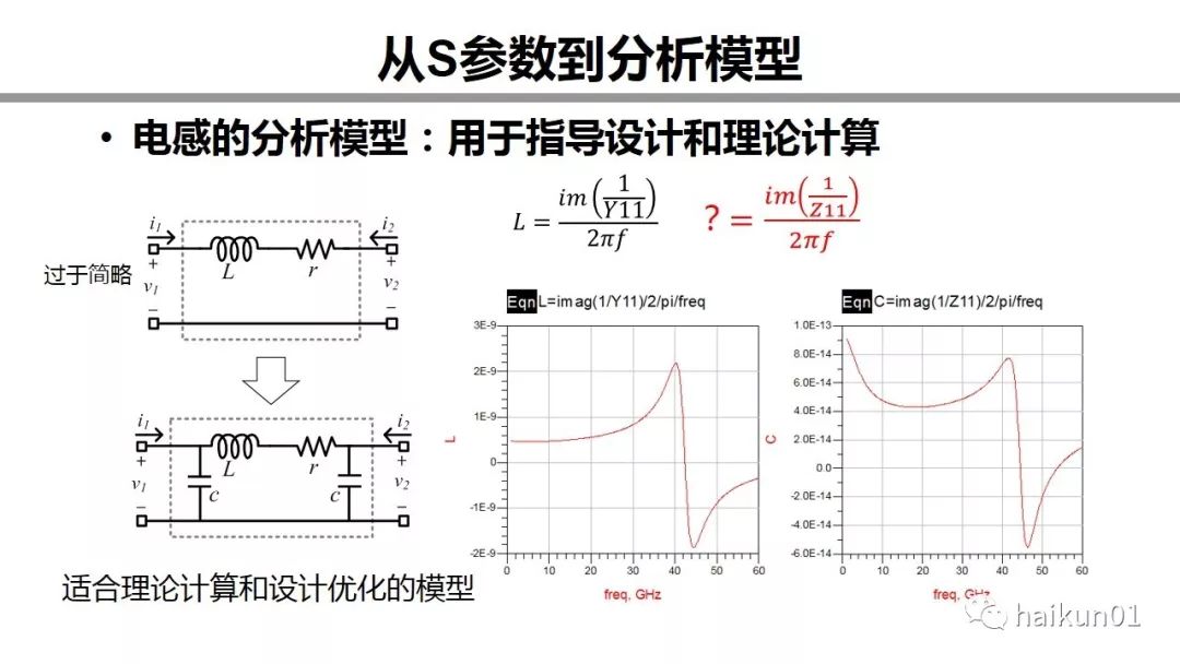
The answer to the first question is here. I think behind the formula L is actually a model that assumes a series of inductors and resistors. Y parameter, 2 ports are short-circuited, the imaginary part is inductive, and the real part is resistive. But in fact, this formula is too simple and completely ignores the capacitance. This is only true when the frequency is much lower than the self-resonant frequency. A model that is most suitable for theoretical calculation and design analysis is the following. So when you look at the imaginary part, what you actually see is the combined effect of inductance and capacitance. If we use the Z parameter, what will be calculated? Z parameter, 2 port open circuit. When the frequency is much lower than the resonance frequency, the inductance is ignored, and the Z parameter basically calculates the parasitic capacitance of the inductance to the ground.
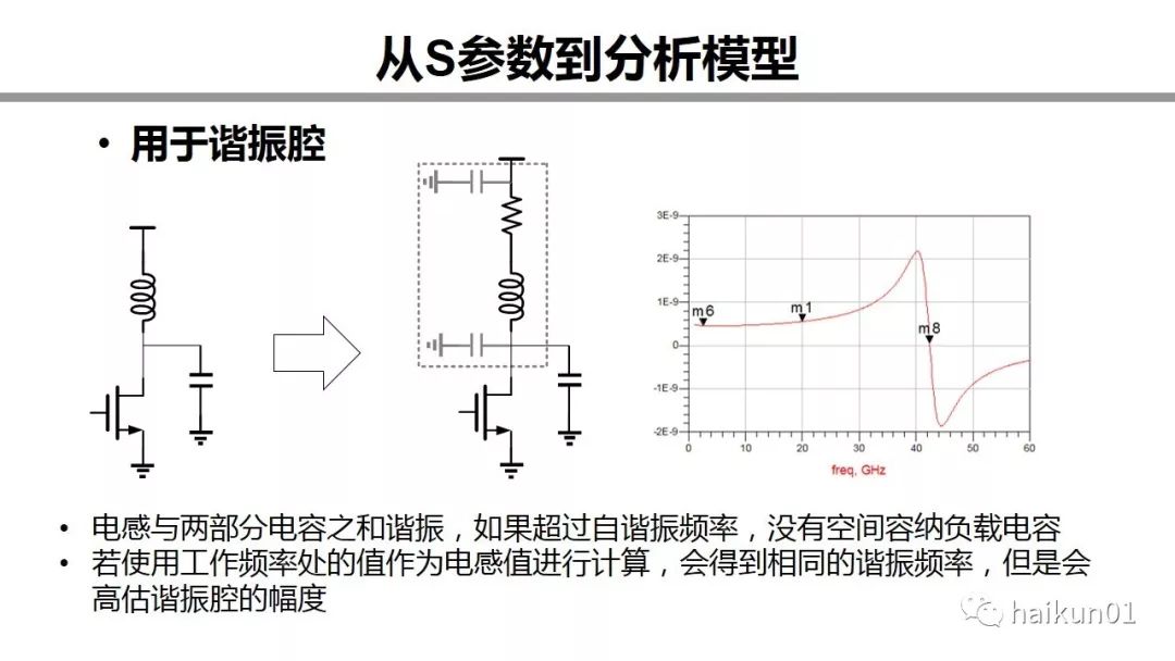
Let us return to the next two questions. Suppose we use inductors for resonant cavity. The inductance actually resonates with the sum of two parts of capacitance, one part is the parasitic of the inductance itself, and the other part is the load capacitance. Therefore, in this case, if the operating frequency is higher than the self-resonant frequency, it means that the inductor has no room for absorbing capacitance at this frequency. If you need to accommodate a smaller load capacitance, the self-resonant frequency can be a little closer to the operating frequency. If the inductance value of the operating frequency is used for theoretical calculation, the resonant frequency obtained should be the same. However, you will overestimate the amplitude of the resonant cavity. The amplitude of the resonant cavity is equal to 2pifL. The values ​​of the operating frequency of this curve are not all inductive values, which is equivalent to taking part of the capacitive as inductive, so the amplitude will be overestimated.
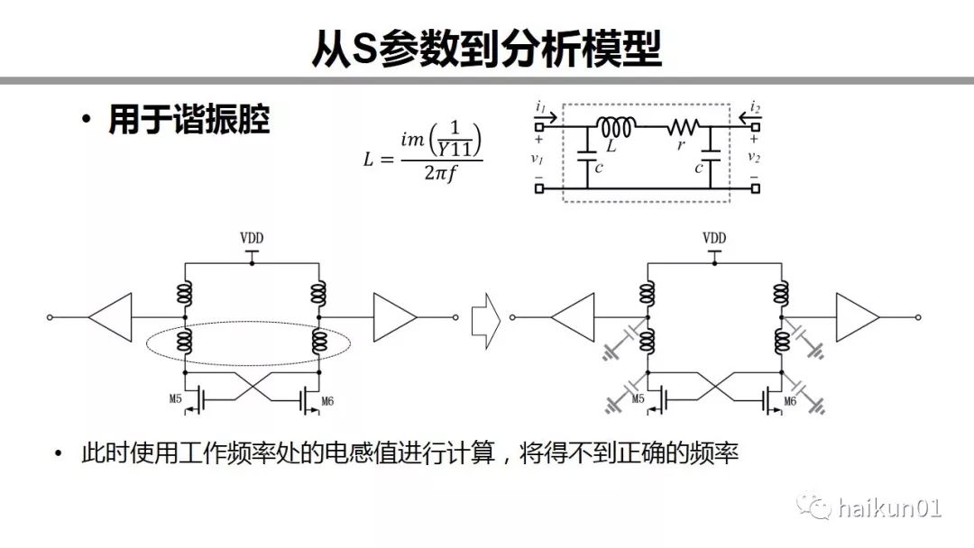
This is another example I have encountered before. I want to imitate such an LCLC network. I first simulated with an ideal component to get the inductance I needed, and then imitated an inductance. The inductance calculated by this formula was the same as the inductance I needed. But one generation close to the circuit, and found that the frequency has dropped a lot. why? When using this formula to calculate the Y parameter, the two terminals are short-circuited, so the capacitance on that side is ignored. But in the LCLC network, this part of the capacitance also has an impact on the circuit.
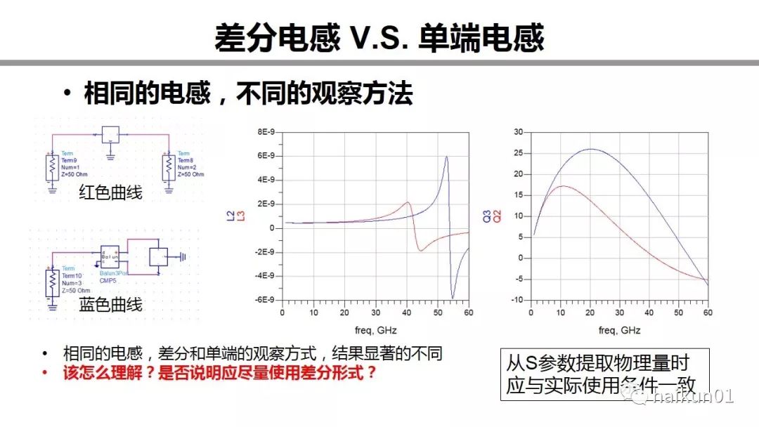
Another is that the same inductance, the structure will be significantly different when viewed in a differential and single-ended way. The DC inductance value is similar, but the self-resonant frequency of the differential is much higher, and the Q value is much higher. Why is this? Does it indicate that differential inductors should be used as much as possible? We will continue to mention it later. When there is a hint, you should be consistent with the actual conditions of use when extracting physical quantities from the S-parameters.
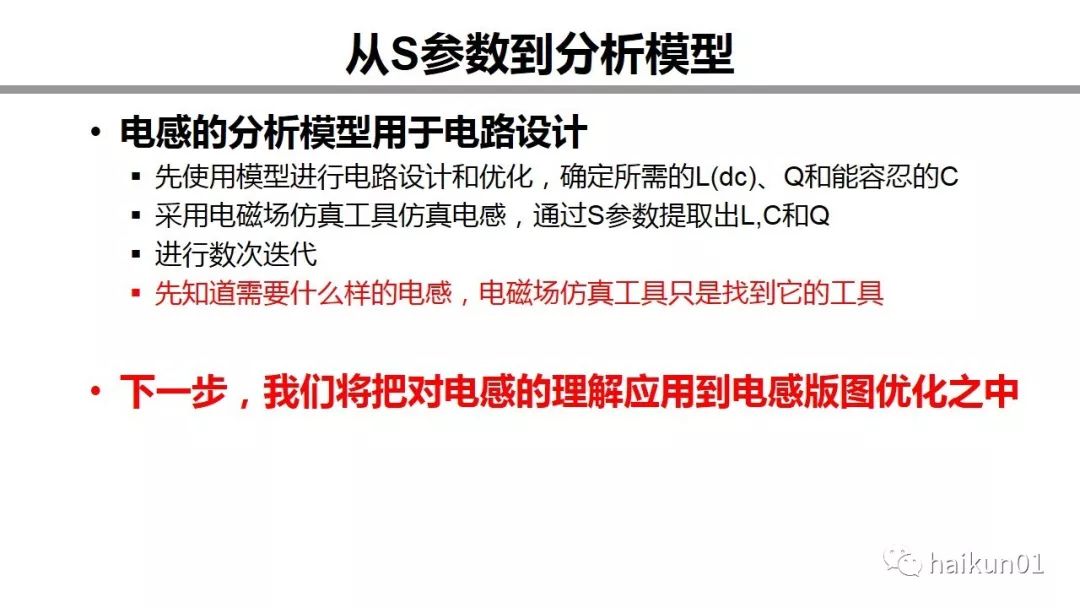
Here is a summary from S-parameters to analysis models. The analysis model is a name that I gave myself to distinguish it from the physical model. When I use inductors to design, I generally use this process. The first step is to simulate and optimize the circuit with an analysis model with capacitors. Determine the inductance value Q I need and the tolerable C. Because you can set these values ​​arbitrarily, you do not need to iterate with HFSS, so the simulation speed in this step will be faster. The second step is to use electromagnetic field to simulate inductance, and extract LC and Q through S parameters. In a word, we must first know what kind of inductance we need. The electromagnetic field simulation tool is just a tool to find it.
Next, I will apply these understandings to the layout optimization of inductors. This is also an example I encountered recently. I think the whole logic is quite interesting and enlightening, so I will share it with you.
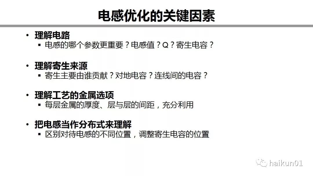
Before looking at specific examples, let's talk about some macro aspects. What are the key factors for inductance optimization? I think there are the following four aspects. The first step is to understand the circuit. Which parameter of the inductance do we require? For example, the Q value of the inductor used to expand the bandwidth is not important. Anyway, a resistor is required at the end, and C is more important. In the VCO and resonant cavity, the Q value is very important. You only need to know which is important before you know how to optimize. The second part is to understand the source of parasitism and who mainly contributes to parasitism. The third step is to understand the metal options of the process, such as how thick each layer of metal is, the layer-to-layer spacing, whether the side parasitic is relatively large or the parasitic to the ground is relatively large. The fourth step is very interesting, the inductor itself is a concentrated component, but when you optimize, you need to treat it as a distributed. The following example can clearly see this.
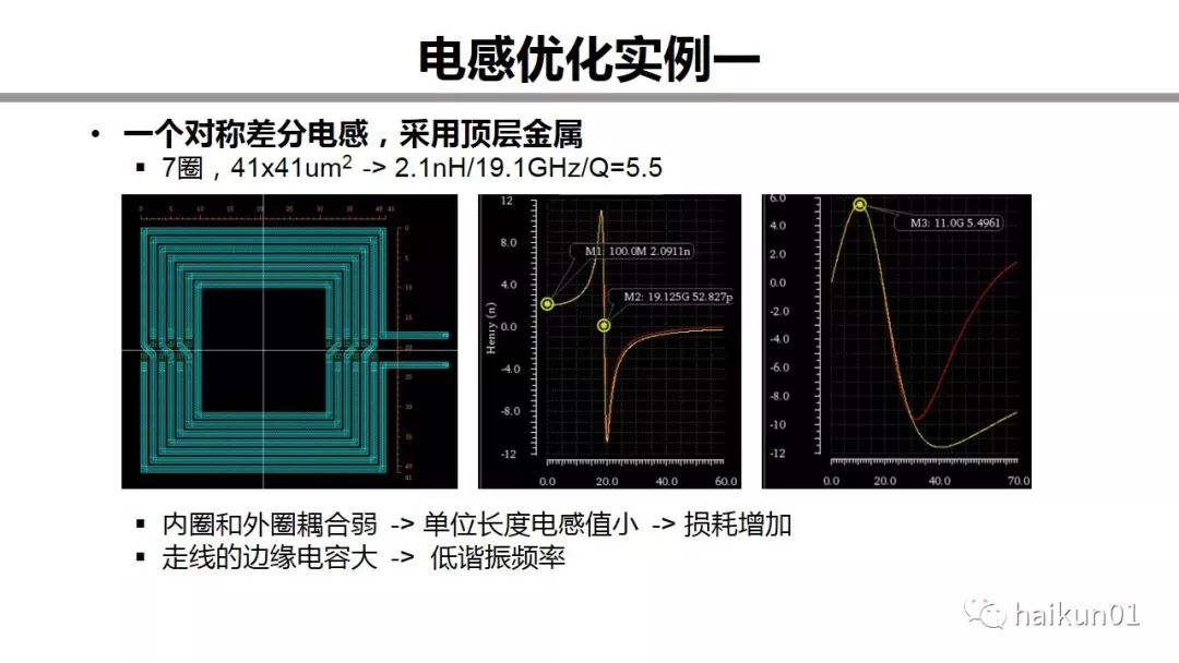
Okay, now let's look at a concrete example. This is a very common symmetrical differential inductor under a certain process. It is wound with top metal and has a total of seven turns. The self-resonant frequency of 2.1nH/19.1G, the Q value of 5.5. Simply think about it, what's the problem with this inductor? First, it has gone around seven times, so the coupling between the outermost circle and the innermost circle is very weak, so the inductance per unit length of the trace is relatively small, so the loss increases. Second, the metal on the top layer is generally thicker, and the rows here are very dense, and the capacitance on the side of the trace is large, so the self-resonant frequency is reduced. How to solve it? A simple method is to increase the line spacing. But the side effect of this is that the coupling between the outer ring and the inner ring is weaker, the inductance density is small, the wiring becomes longer, and the loss becomes larger. Is there no other way?
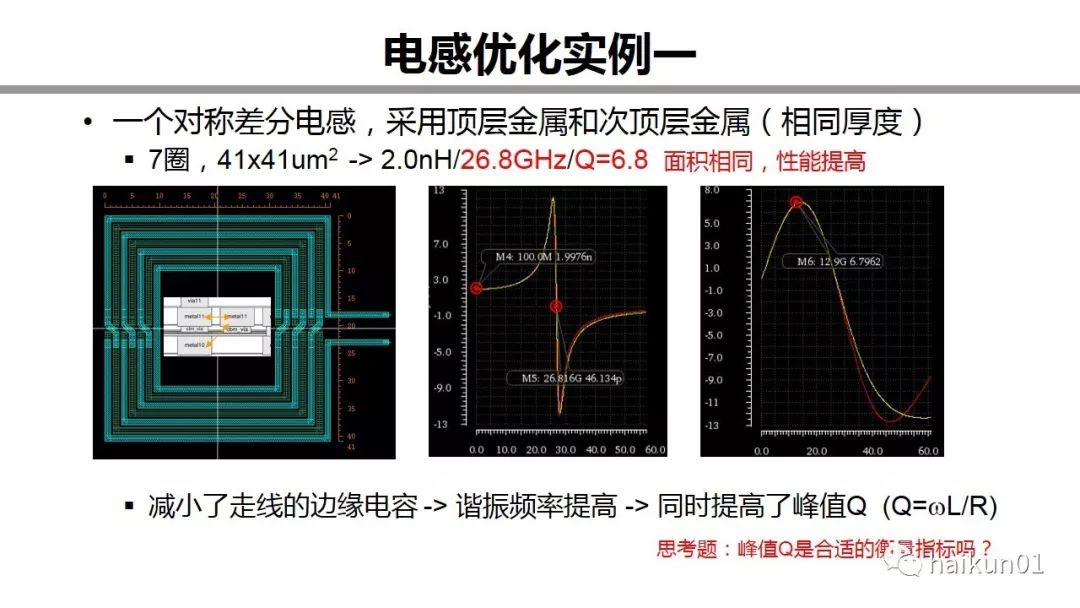
Ok, here I made the first improvement. Make full use of the metal layer provided by the process. Now the inductor is routed with the top layer and the next top layer. Their thickness is the same. Everyone imagine a three-dimensional picture. The second, fourth, and sixth circles are recessed in the three-dimensional diagram, right, so, the edge capacitance of the trace is reduced. The direct benefit is that the resonant frequency has been increased from 19.1G to 26.8G, and the peak Q has also increased from 5.5 to 6.8. . The area has not changed, and the inductance density has not changed. It's like a free benefit.
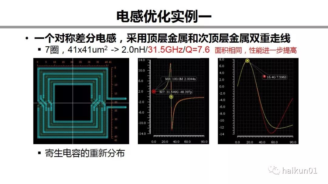
I have carried out the second step of optimization on this page. There are still two layers of metal, the same area, and the same inductance. However, the self-resonant frequency has been further increased from 26.8 to 31.5, and the Q value has been increased from 6.8 to 7.6. There is no cost, and the performance is improved in all directions. In fact, the routing method is optimized here. Don't worry if you don't see this picture clearly. There is a clearer explanation on the next page.
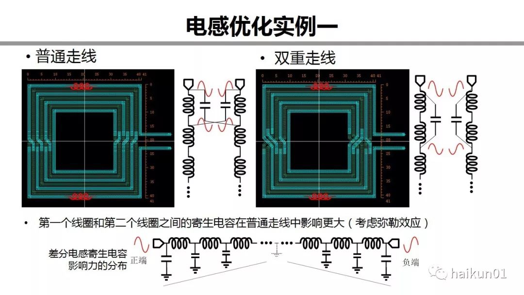
I have drawn two inductors together on this page. Look at this one on the left first. If we regard the half-turn coil as a small inductance, then the outermost half-turn inductance from the positive end, and the half-turn inductance close to it belongs to the negative end. So the parasitic capacitance between them is actually connected across the positive terminal and the negative terminal. What about the double wiring in the picture on the right? By changing the wiring method, starting from the positive end, the inner half-turn inductance of the first half-turn inductance still belongs to the positive end, so the connection position of this parasitic capacitance is changed. Think about the Maitreya effect, in which case this capacitor has a great influence on self-resonance? Obviously it is an ordinary routing. In extreme cases, the capacitance in the left picture should be multiplied by two, and the capacitance in the right picture can be ignored. Therefore, the performance improvement comes from the redistribution of parasitic capacitance.
Here, the differential inductance is drawn in the form of distribution. From both sides to the central virtual spot, the influence of parasitic capacitance is getting smaller and smaller. So when we wind the inductor, we should push it toward the center as much as possible.
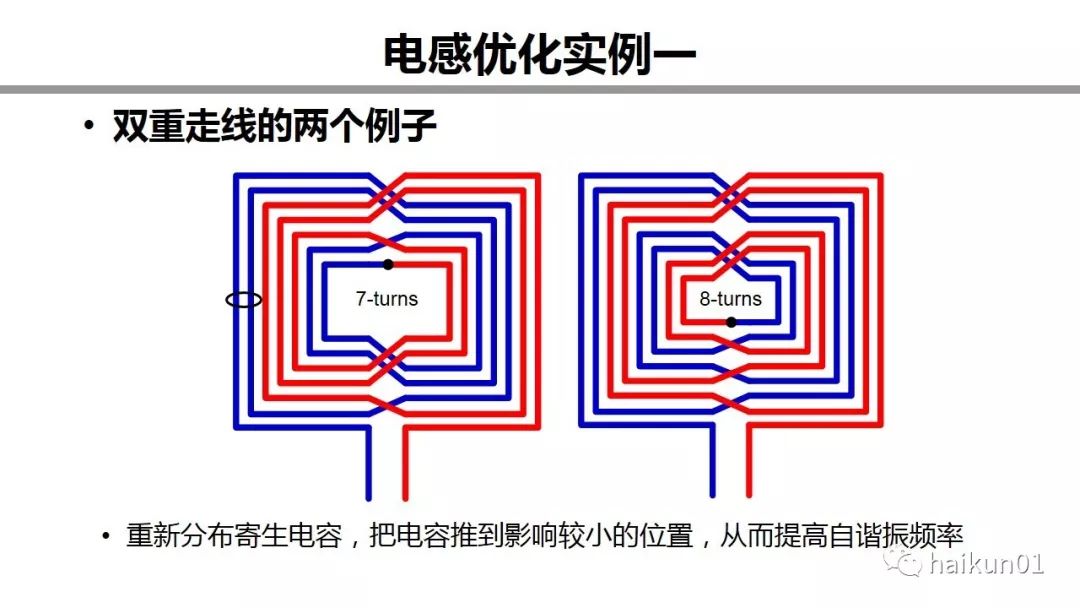
In this picture, I have re-spent the inductance, everyone can take a closer look at how the line goes. It can be seen more clearly.
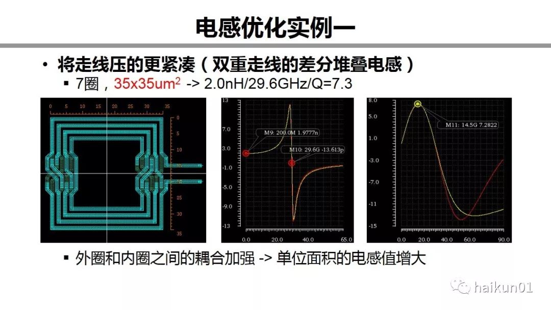
The next step of optimization is to make the wiring more compact, so that the coupling between the outer ring and the inner ring is strengthened, and the inductance density becomes larger. The area has been reduced from 41x41 to 35x35, but at the cost of a small amount of Q at the self-resonant frequency. This is actually a dual-track differential stacked inductor.
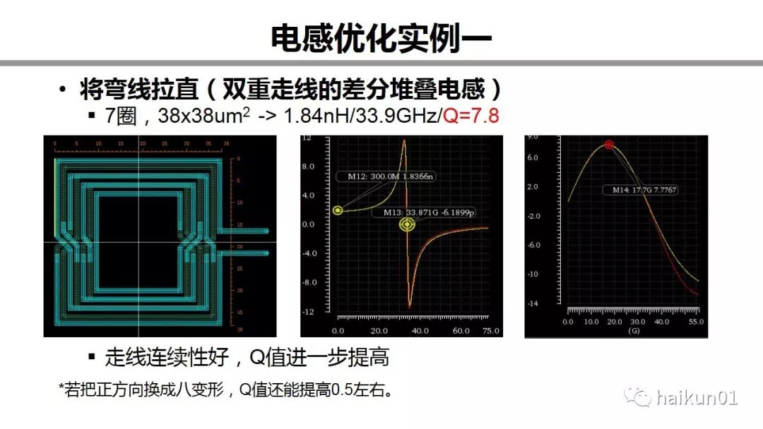
In the last step, I straightened some of the bent wires in the previous inductor. In the end, the inductance decreased, the self-resonant frequency increased to 33.9, and the Q increased to 7.8. If the square is transformed into eight, the Q value can be increased by about 0.5.
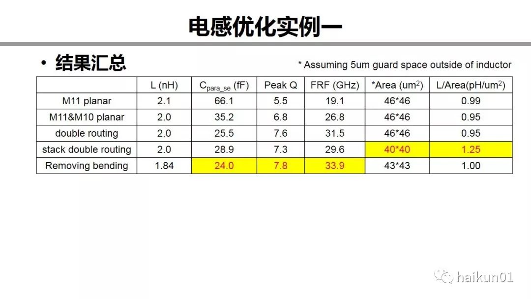
Here are some summaries. As you can see, after we have undergone these optimizations, the performance of the inductor is better than the inductors that have not been optimized before. There is no need to compromise. The price paid is knowledge.
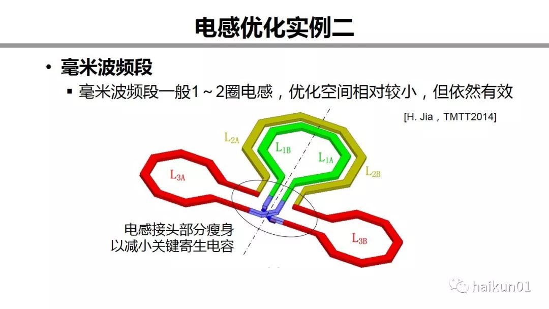
Here is an example of millimeter wave. Millimeter wave inductors generally have fewer turns, so the optimization space is small. But it is still effective. In a design I made, I deliberately made the connector of the inductor connection thinner. This can reduce the parasitic capacitance of key parts. The central part can be made appropriately to reduce the resistance. Because the influence of parasitic resistance at different positions should be consistent.
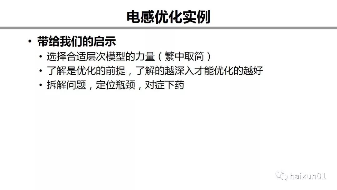
Okay, I want to talk about chicken soup for the soul. This example can actually give us some enlightenment. The first is the power to choose the right level of model. For example, the physical model of the inductor is accurate enough, but it is too complicated. I cannot visually understand the circuit against that. I would rather lose a little accuracy so that I can analyze and understand better. Simplifying the complex is something that an engineer must be able to do. The second revelation is that understanding is the prerequisite for optimization, and the deeper the understanding, the better. If I treat the inductor as a black box and I don’t know what the inside looks like, I can’t optimize it. Only by thinning the inductance into each small segment of the trace can it be better optimized. The third revelation is the way to solve the problem, not only inductance, but any problem. First locate the problem. The low self-resonance frequency means that the parasitic capacitance is large. That is the main source of the parasitic capacitance. If the source is found, it will be easier to handle. I will prescribe the right medicine and push it to an unimportant place.
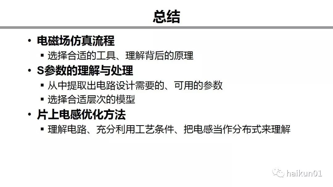
Well, the content shared today probably ends here. Due to time constraints, there are still some points that have not been mentioned. I hope there will be more opportunities to communicate with you in the future. I hope that today's content will give you some inspiration.
Portable high efficient travel charger, can charge multi devices at the same time, every port output mini 5v 1a, max 5v 2.1a. We can meet your specific requirement of the products, like label design. The plug type is US/UK/AU/EU. The material of this product is PC+ABS. All condition of our product is 100% brand new.
Our products built with input/output overvoltage protection, input/output overcurrent protection, over temperature protection, over power protection and short circuit protection. You can send more details of this product, so that we can offer best service to you!
Usb Charger,Universal Travel Adapter,Intelligent Usb Charger,Travel Adapter
Shenzhen Waweis Technology Co., Ltd. , https://www.huaweishiadapter.com