The subject recently started to work on the work related to FPGA verification, and needs to grasp the detailed information of the internal resources of the FPGA, so I carefully reviewed the official device manual. This time, the content shared by everyone mainly involves CLBs, SelecTIO and Clocking resources in Xilinx FPGA. It is suitable for friends who have timing requirements for FPGA design but have not enough enough to understand.
On the reference device, although some dedicated resources are concentrated in the high-end FPGA models, but the main idea, or put them in the follow-up article of the series. The evidence in the following is from the Spartan6 device documentation, so it will not exceed the Spartan6 coverage.
The traditional FPGA internal resources are classified into three categories: Configurable Logic Block, Input Output Block and Interconnect. These are all known. With the development of FPGAs, in order to meet the needs of signal processing and on-chip storage, block RAM (BRAM), clock management unit and hardware multiplier have been added to the first three categories, and then PPC and High-speed serial input and output, and more.
In the CLB, SelecTIO, and Clocking resources that will be mentioned below, the SelecTIO resource is a relatively rich class, so put it in the end in order.
text:Let's talk about CLB first. It is one of the most important and actually the easiest to use structures. Xilinx opens up as many resource configuration interfaces as possible to users, but CLB is not one of them to control the development cycle and improve system stability. Its configuration scheme is almost entirely distributed by IDE to process intelligence, users can constrain The location of the special slice, but rarely this is necessary, it will be more effective to give the IDE to complete.
Let's take a look at its structure (some pictures are not easy to find, and will be completed when the integration is completed):
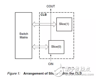
1 CLB resources are divided into several areas by the internal clock network according to the size of the FPGA, generally 40 areas of each CLB unit height;
2 Each CLB is connected to a switch matrix to access the global routing matrix;
3 A CLB unit contains a pair of Slice cells (two slices are not directly connected and are arranged in columns between CLBs, and each column has a separate carry chain);
4 The slice in the lower part of a CLB is recorded as Slice0, and the upper part is recorded as Slice1;
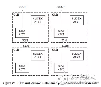
5 Each slice contains 4 lookup tables (LUTs), 8 memory locations (FF), and some selector and carry logic for providing logic, arithmetic, and ROM functions;
6 Some Slices support DistributedRAM and 32-bit shift register functions, which are denoted as SLICEM, others are referred to as SLICEL (a CLB has at most one SLICEM, and each CLB column has at least one SLICEM in DSP48E (hardware multiplication in Xilinx FPGA) The two CLB columns next to the column, each CLB has SLICEM).
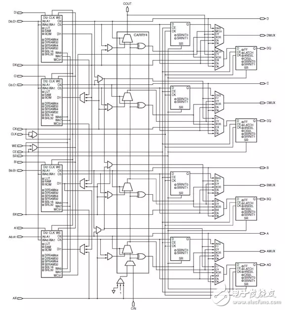
SLICEM
(DistributedRAM and ShiftRegisters resources are all mounted on LUTs)
Finally, take a look at the total amount of resources in a CLB:

Of course, there are some details about the several resources in Slice that need attention, mainly related to the characteristics of LUTs, but let's join the case later. If you have some experience and experience with FPGA design before, now you must have your own understanding of the FPGA lookup table structure.
Or simply mention the role of LUTs, is to look up the table,, in my opinion, it is a 6-input and 2-output multi-function selector that can directly map the behavior of the always block in Verilog to its behavior, through With the connection configuration of the input port, it is able to implement the signal behavior model we need. The complete process will be added to the case later. Let us take a breath and go to the next content.
Xilinx FPGA has a complex network of clock resources to maintain timing requirements and system stability under a large number of logical resources. It is mainly divided into a global clock line and a local clock network. On Spartan6, there are two hard core resources, a digital clock manager (DCM) and a digital phase-locked loop (PLL), to assist the clock resource network. Spartan6 internally provides 16 global clock-driven buffers and 40 local clocks, which are evenly distributed among the various regions segmented by the clock network mentioned above:
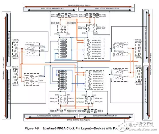
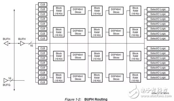
We can call these resources by instantiating primitives such as BUFG and BUFIO to provide a lower phase offset clock reference for high-speed signal groups such as GTP (H/X/Z) and DDR, AD/DA, but the allocation of clock resources. There are a lot of usage rules, and when the resources are limited and the wiring is tight, the Xilinx rule checker is often notified of the use violation. After that, the subject will combine some real cases to guide everyone to avoid such mistakes.
The space used for clock resources is also very short. In fact, there are many problems related to the clock, but it is valuable to know when you need it. Otherwise, there is no basis for understanding and there is no value. Next, let's take a look at the most abundant I/O resources inside the FPGA. After all, the most extensive and best-selling FPGA on the market today is the interface. The following contains a lot of content, which is almost the same specification on multiple series of FPGAs:
1 FPGA I / O resources are distributed in several banks, there are 20 I / O TIle in each bank;
2 One Tile contains 2 IOBs, 2 ILOGICs, 2 OLOGICs and 2 IOEDLAYs for pairing double-ended (differential) signals;
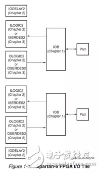
3 IOB contains input, output and tri-state drivers, which can be configured as different I/O standards; IOB directly connects a pair of I(O)LOGIC, I(O)LOGIC contains logical resources and three-state control of data I/O. I(O)LOGIC can also be configured as I(O)SERDES by calling related primitives to implement serial-to-parallel conversion of data;
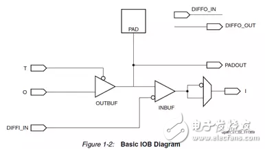
The IOB unit supports a large number of interface standards to control load capacity and slew rate. And the same voltage output is supported in the same bank to drive some low voltage I/O standards, but there are some rules for the selection of the reference level.
For single-ended and dual-ended signal I/O, you can choose a variety of buffer configuration methods to drive these signals. Of course, the implementation of the IDE also helps us configure a lot. As a user, commonly used clock drivers like IBUFG and IBUFR. Resources, IBUFDS, OBUFDS to achieve single-ended conversion of signals, and three-state control with OBUFT.
ZGAR Aurora 2500 Puffs
ZGAR electronic cigarette uses high-tech R&D, food grade disposable pod device and high-quality raw material. All package designs are Original IP. Our designer team is from Hong Kong. We have very high requirements for product quality, flavors taste and packaging design. The E-liquid is imported, materials are food grade, and assembly plant is medical-grade dust-free workshops.
Our products include disposable e-cigarettes, rechargeable e-cigarettes, rechargreable disposable vape pen, and various of flavors of cigarette cartridges. From 600puffs to 5000puffs, ZGAR bar Disposable offer high-tech R&D, E-cigarette improves battery capacity, We offer various of flavors and support customization. And printing designs can be customized. We have our own professional team and competitive quotations for any OEM or ODM works.
We supply OEM rechargeable disposable vape pen,OEM disposable electronic cigarette,ODM disposable vape pen,ODM disposable electronic cigarette,OEM/ODM vape pen e-cigarette,OEM/ODM atomizer device.

Aurora 2500 Puffs,ZGAR Aurora 2500 Puffs Pod System Vape,ZGAR Aurora 2500 Puffs Pos Systems Touch Screen,ZGAR Aurora 2500 Puffs Disposable Vape Pod System,2500Puffs Pod Vape System
ZGAR INTERNATIONAL(HK)CO., LIMITED , https://www.szvape-pods.com