Abstract: This in-depth arTIcle covers the theory behind a Delta-Sigma analog-to-digital converter (ADC). It specifically focuses on the difficult to understand key digital concepts of over-sampling, noise shaping, and decimaTIon filtering. A descripTIon of new converter, the MAX1402, and several applicaTIons for Delta-Sigma converters are included.
Sigma-delta converters offer high resolution, high integration, and low cost, making them a good ADC choice for applications such as process control and weighing scales. Designers often choose a classic SAR ADC instead, because they don't understand the sigma-delta types.
The analog side of a sigma-delta converter (a 1-bit ADC) is very simple. The digital side, which is what makes the sigma-delta ADC inexpensive to produce, is more complex. It performs filtering and decimation. To understand how it works, you must become familiar with the concepts of oversampling, noise shaping, digital filtering, and decimation.
This application note covers these topics. OversamplingFirst, consider the frequency-domain transfer function of a traditional multi-bit ADC with a sine-wave input signal. This input is sampled at a frequency Fs. According to Nyquist theory, Fs must be at least twice the bandwidth of the input signal.
When observing the result of an FFT analysis on the digital output, we see a single tone and lots of random noise extending from DC to Fs / 2 (Figure 1). Known as quantization noise, this effect results from the following consideration: the ADC input is a continuous signal with an infinite number of possible states, but the digital output is a discrete function whose number of different states is determined by the converter's resolution. So, the conversion from analog to digital loses some information and introduces some distortion into the signal. The magnitude of this error is random, with values ​​up to ± LSB.
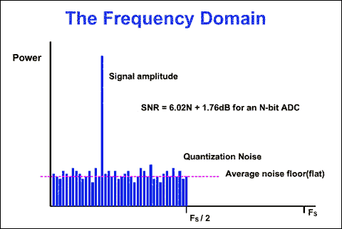
Figure 1. FFT diagram of a multi-bit ADC with a sampling frequency FS.
If we divide the fundamental amplitude by the RMS sum of all the frequencies representing noise, we obtain the signal to noise ratio (SNR). For an N-bit ADC, SNR = 6.02N + 1.76dB. To improve the SNR in a conventional ADC (and consequently the accuracy of signal reproduction) you must increase the number of bits.
Consider again the above example, but with a sampling frequency increased by the oversampling ratio k, to kFs (Figure 2). An FFT analysis shows that the noise floor has dropped. SNR is the same as before, but the noise energy has been spread over a wider frequency range. Sigma-delta converters exploit this effect by following the 1-bit ADC with a digital filter (Figure 3). The RMS noise is less, because most of the noise passes through the digital filter. This action enables sigma -delta converters to achieve wide dynamic range from a low-resolution ADC.
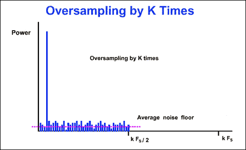
Figure 2. FFT diagram of a multi-bit ADC with a sampling frequency kFS.
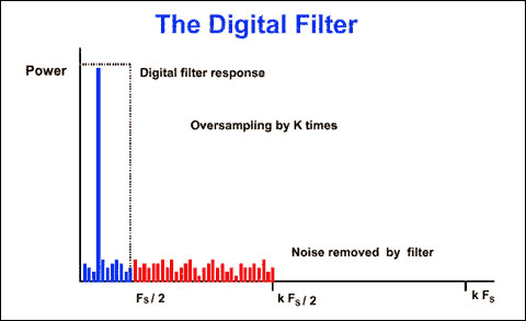
Figure 3. Effect of the digital filter on the noise bandwidth.
Does the SNR improvement come simply from oversampling and filtering? Note that the SNR for a 1-bit ADC is 7.78dB (6.02 + 1.76). Each factor-of-4 oversampling increases the SNR by 6dB, and each 6dB increase is equivalent to gaining one bit. A 1-bit ADC with 24x oversampling achieves a resolution of four bits, and to achieve 16-bit resolution you must oversample be a factor of 415, which is not realizable. But, sigma-delta converters overcome this limitation with the technique of noise shaping, which enables a gain of more than 6dB for each factor of 4x oversampling. Noise ShapingTo understand noise shaping, consider the block diagram of a sigma-delta modulator of the first order (Figure 4). It includes a difference amplifier, an integrator, and a comparator with feedback loop that contains a 1-bit DAC. (This DAC is simply a switch that connects the negative input of the difference amplifier to a positive or a negative reference voltage.) The purpose of the feedback DAC is to maintain t he average output of the integrator near the comparator's reference level.
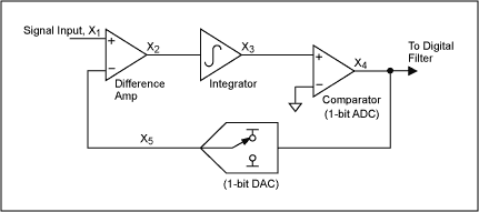
Figure 4. Block diagram of a sigma-delta modulator.
The density of "ones" at the modulator output is proportional to the input signal. For an increasing input the comparator generates a greater number of "ones," and vice versa for a decreasing input. By summing the error voltage, the integrator acts as a lowpass filter to the input signal and a highpass filter to the quantization noise. Thus, most of the quantization noise is pushed into higher frequencies (Figure 5). Oversampling has changed not the total noise power, but its distribution.
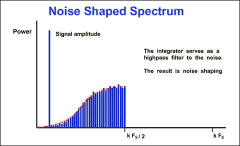
Figure 5. Affect of the integrator in the sigma-delta modulator.
If we apply a digital filter to the noise-shaped delta-sigma modulator, it removes more noise than does simple oversampling (Figure 6). This type of modulator (first-order) provides a 9dB improvement in SNR for every doubling of the sampling rate. For higher orders of quantization, we can achieve noise shaping by including more than one stage of integration and summing in the sigma-delta modulator. For example, the second-order sigma-delta modulator of Figure 7 provides a 15dB improvement in SNR for every doubling of the sampling rate. Figure 8 shows the relationship between the order of the sigma-delta modulator and the amount of over-sampling necessary to achieve a particular SNR.
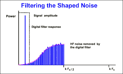
Figure 6. Effect of the digital filter on the shaped noise.
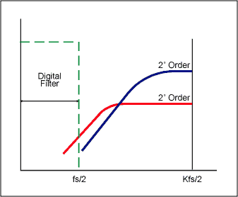
Figure 7. Using more than one integrator and summing stage to achieve a higher order of quantization noise.
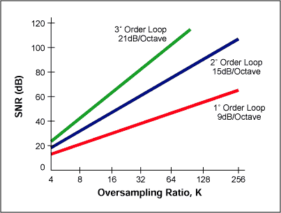
Figure 8. Relationship between order of sigma-delta modulator and the amount of over-sampling necessary to achieve a particular SNR. Digital and Decimation FilterThe output of the sigma-delta modulator is a 1-bit data stream at the sampling rate, which can be in the megahertz range. The purpose of the digital-and-decimation filter (Figure 9) is to extract information from this data stream and reduce the data rate to a more useful value. In a sigma-delta ADC, the digital filter averages the 1-bit data stream, improves the ADC resolution, and removes quantization noise that is outside the band of interest. It determines the signal bandwidth, settling time, and stopband rejection.

Figure 9. Digital side of sigma-delta modulator.
In sigma-delta converters, a widely used filter topology that performs the lowpass function is the Sinc³ type (Figure 10). The main advantage of this filter is its notch response, which (for example) can reject the line frequency when set at that frequency. The notch position is directly related to the output data rate (1 / data-word period). The SINC³ filter settles in three data-word periods. With a 60Hz notch (60Hz data rate) the settling time is 3 / 60Hz = 50ms. For applications that require lower resolution and a faster settling time, consider an ADC of the MAX1400 family, which gives you a choice of filter type (SINC¹ or SINC³).
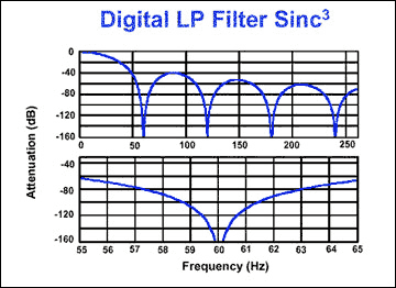
Figure 10. Low-pass function performed by Sinc³ filter.
The settling time of a SINC¹ filter is one data word. As in the example above, 1 / 60Hz = 16.7ms. Because bandwidth is reduced by the digital output filter, the output data rate can satisfy the Nyquist criterion even though it is lower than the original sampling rate. This can be accomplished by preserving certain input samples and discarding the rest. This process is known as decimation by a factor of M (the decimation ratio). M can have any integer value, provided that the output data rate is more than twice the signal bandwidth (Figure 11). If the input has been sampled at fs, the filtered-output data rate can therefore be reduced to fs / M without loss of information.
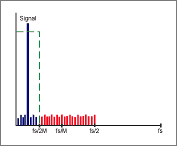
Figure 11. Decimation does not cause any loss of information.
New Sigma-Delta ADCs from MaximRecent highly integrated sigma-delta ADCs manage small signals with a minimum number of external components. As an example of this new generation, the MAX1402 chip includes so many functions that it can be called a system-on-a -chip (Figure 12). Drawing a low quiescent current of 250µA in operating mode (2µA in power-down mode), it provides 16-bit accuracy at 480sps and 12-bit accuracy at 4800sps.
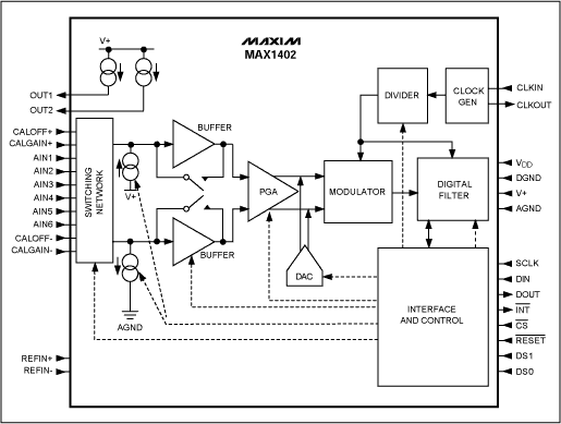
Figure 12. MAX1402 block diagram.
The MAX1402 signal chain consists of the following: a flexible input multiplexer that can be set to manage three fully differential signals or five pseudo-differential signals, two chopper amplifiers, a programmable PGA (with gain from 1 to 128), a coarse DAC to remove system offset, and a second-order sigma-delta modulator. The 1-bit data stream is then filtered with an integrated digital filter configurable as SINC¹ or SINC³. The conversion result is made available via an SPI ™ / QSPI ™ -compatible, 3-wire serial interface.
The chip also includes two fully differential input channels for calibration of offset and gain, two matched 200µA transducer-excitation currents (suitable for 3-wire and 4-wire RTD applications), and two "burn-out" currents for testing the integrity of the selected transducer. The device is programmed via the serial interface to access the eight internal registers that select the mode of operation. Setting the SCAN control bit enables the chip to read the input channel either on demand or continually, and the input channel is identified by a 3-bit "channel identification" attached to each conversion result.
Figure 13 establishes the correct input voltage range, which is defined by the U / B-bar bit, Vref, PGA, and DAC settings. No offset action is performed when the DAC code equals "0000." With Vref = 2.5V, for example, a full scale of 0V to 5V can be accommodated by setting the DAC to "1110," the PGA to "000," and the U / B-bar bit to "0."
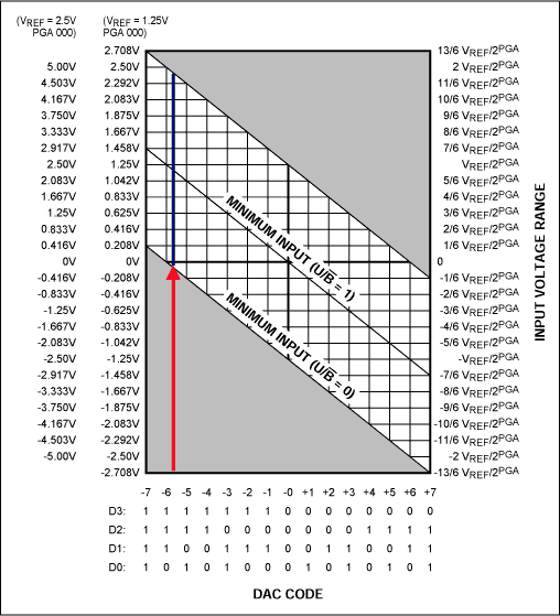
Figure 13. MAX1402 input voltage-range setting.
The two calibration channels (CALOFF and CALGAIN) can be used to correct the measurement. For this purpose, CALOFF inputs are connected to ground and CALGAIN inputs are connected to the reference voltage. The averaged measurements performed on these channels are used in the following interpolation formula: Voltage = [Vref × (Code-CALOFF code)] / [(CALGAIN code-CALOFF code) × PGA gain]. Application of Sigma-Delta ADCs Thermocouple Measurement with Cold-Junction CompensationTo eliminate noise pickup from the thermocouple leads, the MAX1402 in this application (Figure 14) uses the buffered mode to allow large decoupling capacitors on the front end. Due to the reduced common-mode range available in this mode, it is necessary to bias the AIN2 input at the reference voltage (2.5V ). Thermocouple measurements present the problem of a thermoelectric potential, created by connecting the thermocouple probe to the measurement instrument. This potential introduces a temperature-dependent error that must be subtracted from the temperature measurement to obtain an accurate result.
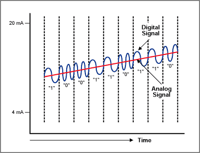
Figure 14. Thermocouple measurement with cold-junction compensation.
Voltage measured by the instrument can be expressed as α (T1-Tref), where α is the Seebeck constant for the thermocouple, T1 is the temperature being measured, and Tref is the temperature of the junction block. To compensate the Seebeck coefficient, you can add (to the thermocouple output) a portion of the temperature-dependent voltage developed by a diode, or you can acquire the junction-block temperature and calculate the compensation with software. In that arrangement, the pn-junction temperature is measured by the differential input channel AIN3-AIN4, biased by the 200µA internal current generator.
3-Wire and 4-Wire RTD ConfigurationThe demanding temperature measurements required in process control favor platinum resistance temperature detectors (RTDs) because of their excellent accuracy and interchangeability. A platinum RTD produces 100Ω at 0 ° C and 200Ω at + 266 ° C. The sensitivity of the RTD is very low (ΔR / ΔT = 100Ω / 266 ° C), and an applied excitation current of 200µA produces 20mV at 0 ° C and 40mV at + 266 ° C. These signal levels can be handled directly by the MAX1402's analog input.
The measurement accuracy can be affected by errors due to wiring resistance. You can use a traditional 2-wire configuration when the RTD is located near the converter, but when it is located remotely, the wiring resistance can cause significant error by adding to the RTD impedance. Three-wire and 4-wire RTD configurations should be used for these types of installation.
The two matched 200µA current sources enable compensation of the errors in 3-wire and 4-wire RTD configurations. In the 3-wire case (Figure 15), these current sources, flowing in RL1 and RL2, ensure that the differential voltage at AIN1 -AIN2 is not affected by lead resistance. This holds true provided both leads are of the same material and of equal length (RL1 = RL2), and that the current sources have finely matched tempcos (the MAX1402 tempco is 5ppm / ° C).
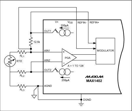
Figure 15. 3-Wire RTD application.
The 4-wire configuration has no lead-resistance error because no current flows in the measurement leads connected to AIN1 and AIN2 (Figure 16). Current source OUT1 provides excitation current for the RTD, and current source OUT2 provides current to generate the reference voltage . The ratiometric configuration ensures that RTD tempco errors (due to temperature drift in the RTD current source) are compensated by variation in the reference voltage.
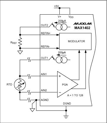
Figure 16. 4-Wire RTD application.
Smart 4-20mA TransmitterIn the old-fashioned 4-20mA transmitter, a field-mounted device senses a physical parameter such as pressure or temperature, and generates (in the standard 4-20mA range) a current proportional to the measured variable. Current loops provide advantages: the measurement signal is insensitive to noise, and power can be derived from a remotely supplied voltage. In response to industry demand, the second generation of 4-20mA transmitters (called "smart" transmitters) were developed to condition the signal remotely , using a microprocessor and data converters.
Smart devices can normalize gain and offset, and they linearize sensors such as RTDs and thermocouples by converting to digital, processing with arithmetic algorithms in the µP, converting back to analog, and transmitting a standard current via the loop (Figure 17). Third- generation "smart and intelligent" 4-20mA transmitters add (to the smart device) digital communications that share the twisted-pair line with the 4-20mA signal. This communication channel also allows transmission of control and diagnostic signals. A low-power device such as the MAX1402 is suitable because its 250µA supply current saves considerable power for the remaining transmitter circuitry.
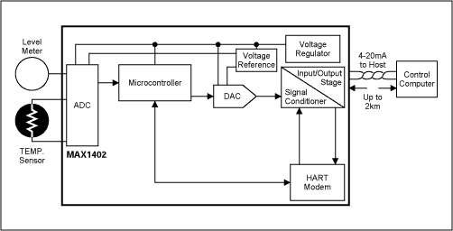
Figure 17. Intelligent 4-20mA transmitter.
The communication standard for smart transmitters is the HART protocol. Based on the Bell 202 telephone communication standard, HART employs the frequency shift keying (FSK) principle. The digital signal consists of two frequencies representing 1 and 0 (1200Hz and 2200Hz). To provide simultaneous analog and digital communications, sine waves at these frequencies are superimposed on the DC analog-signal cables (Figure 18). Because the average value of the FSK signal is always zero, it does not affect the 4-20mA analog signal. Response time for the digital communication signal allows approximately 2-3 data updates per second without interrupting the analog signal. A minimum loop impedance of 23Ω is required for communication.

Figure 18. Simultaneous analog and digital communication. SummaryBefore the advent of highly integrated conditioning systems, process control was implemented using several independent chips for signal conditioning and processing. As an alternative, the Sigma-Delta approach lowers cost while minimizing the board space and power supply requirements (many applications require only a single 3V or 5V supply). Single-supply operation is particular suitable for battery-powered portable systems, and fewer components improves the system reliability.
A similar version of this article appeared in the August 2002 issue of Sensors magazine.
Sigma-delta converters offer high resolution, high integration, and low cost, making them a good ADC choice for applications such as process control and weighing scales. Designers often choose a classic SAR ADC instead, because they don't understand the sigma-delta types.
The analog side of a sigma-delta converter (a 1-bit ADC) is very simple. The digital side, which is what makes the sigma-delta ADC inexpensive to produce, is more complex. It performs filtering and decimation. To understand how it works, you must become familiar with the concepts of oversampling, noise shaping, digital filtering, and decimation.
This application note covers these topics. OversamplingFirst, consider the frequency-domain transfer function of a traditional multi-bit ADC with a sine-wave input signal. This input is sampled at a frequency Fs. According to Nyquist theory, Fs must be at least twice the bandwidth of the input signal.
When observing the result of an FFT analysis on the digital output, we see a single tone and lots of random noise extending from DC to Fs / 2 (Figure 1). Known as quantization noise, this effect results from the following consideration: the ADC input is a continuous signal with an infinite number of possible states, but the digital output is a discrete function whose number of different states is determined by the converter's resolution. So, the conversion from analog to digital loses some information and introduces some distortion into the signal. The magnitude of this error is random, with values ​​up to ± LSB.

Figure 1. FFT diagram of a multi-bit ADC with a sampling frequency FS.
If we divide the fundamental amplitude by the RMS sum of all the frequencies representing noise, we obtain the signal to noise ratio (SNR). For an N-bit ADC, SNR = 6.02N + 1.76dB. To improve the SNR in a conventional ADC (and consequently the accuracy of signal reproduction) you must increase the number of bits.
Consider again the above example, but with a sampling frequency increased by the oversampling ratio k, to kFs (Figure 2). An FFT analysis shows that the noise floor has dropped. SNR is the same as before, but the noise energy has been spread over a wider frequency range. Sigma-delta converters exploit this effect by following the 1-bit ADC with a digital filter (Figure 3). The RMS noise is less, because most of the noise passes through the digital filter. This action enables sigma -delta converters to achieve wide dynamic range from a low-resolution ADC.

Figure 2. FFT diagram of a multi-bit ADC with a sampling frequency kFS.

Figure 3. Effect of the digital filter on the noise bandwidth.
Does the SNR improvement come simply from oversampling and filtering? Note that the SNR for a 1-bit ADC is 7.78dB (6.02 + 1.76). Each factor-of-4 oversampling increases the SNR by 6dB, and each 6dB increase is equivalent to gaining one bit. A 1-bit ADC with 24x oversampling achieves a resolution of four bits, and to achieve 16-bit resolution you must oversample be a factor of 415, which is not realizable. But, sigma-delta converters overcome this limitation with the technique of noise shaping, which enables a gain of more than 6dB for each factor of 4x oversampling. Noise ShapingTo understand noise shaping, consider the block diagram of a sigma-delta modulator of the first order (Figure 4). It includes a difference amplifier, an integrator, and a comparator with feedback loop that contains a 1-bit DAC. (This DAC is simply a switch that connects the negative input of the difference amplifier to a positive or a negative reference voltage.) The purpose of the feedback DAC is to maintain t he average output of the integrator near the comparator's reference level.

Figure 4. Block diagram of a sigma-delta modulator.
The density of "ones" at the modulator output is proportional to the input signal. For an increasing input the comparator generates a greater number of "ones," and vice versa for a decreasing input. By summing the error voltage, the integrator acts as a lowpass filter to the input signal and a highpass filter to the quantization noise. Thus, most of the quantization noise is pushed into higher frequencies (Figure 5). Oversampling has changed not the total noise power, but its distribution.

Figure 5. Affect of the integrator in the sigma-delta modulator.
If we apply a digital filter to the noise-shaped delta-sigma modulator, it removes more noise than does simple oversampling (Figure 6). This type of modulator (first-order) provides a 9dB improvement in SNR for every doubling of the sampling rate. For higher orders of quantization, we can achieve noise shaping by including more than one stage of integration and summing in the sigma-delta modulator. For example, the second-order sigma-delta modulator of Figure 7 provides a 15dB improvement in SNR for every doubling of the sampling rate. Figure 8 shows the relationship between the order of the sigma-delta modulator and the amount of over-sampling necessary to achieve a particular SNR.

Figure 6. Effect of the digital filter on the shaped noise.

Figure 7. Using more than one integrator and summing stage to achieve a higher order of quantization noise.

Figure 8. Relationship between order of sigma-delta modulator and the amount of over-sampling necessary to achieve a particular SNR. Digital and Decimation FilterThe output of the sigma-delta modulator is a 1-bit data stream at the sampling rate, which can be in the megahertz range. The purpose of the digital-and-decimation filter (Figure 9) is to extract information from this data stream and reduce the data rate to a more useful value. In a sigma-delta ADC, the digital filter averages the 1-bit data stream, improves the ADC resolution, and removes quantization noise that is outside the band of interest. It determines the signal bandwidth, settling time, and stopband rejection.

Figure 9. Digital side of sigma-delta modulator.
In sigma-delta converters, a widely used filter topology that performs the lowpass function is the Sinc³ type (Figure 10). The main advantage of this filter is its notch response, which (for example) can reject the line frequency when set at that frequency. The notch position is directly related to the output data rate (1 / data-word period). The SINC³ filter settles in three data-word periods. With a 60Hz notch (60Hz data rate) the settling time is 3 / 60Hz = 50ms. For applications that require lower resolution and a faster settling time, consider an ADC of the MAX1400 family, which gives you a choice of filter type (SINC¹ or SINC³).

Figure 10. Low-pass function performed by Sinc³ filter.
The settling time of a SINC¹ filter is one data word. As in the example above, 1 / 60Hz = 16.7ms. Because bandwidth is reduced by the digital output filter, the output data rate can satisfy the Nyquist criterion even though it is lower than the original sampling rate. This can be accomplished by preserving certain input samples and discarding the rest. This process is known as decimation by a factor of M (the decimation ratio). M can have any integer value, provided that the output data rate is more than twice the signal bandwidth (Figure 11). If the input has been sampled at fs, the filtered-output data rate can therefore be reduced to fs / M without loss of information.

Figure 11. Decimation does not cause any loss of information.
New Sigma-Delta ADCs from MaximRecent highly integrated sigma-delta ADCs manage small signals with a minimum number of external components. As an example of this new generation, the MAX1402 chip includes so many functions that it can be called a system-on-a -chip (Figure 12). Drawing a low quiescent current of 250µA in operating mode (2µA in power-down mode), it provides 16-bit accuracy at 480sps and 12-bit accuracy at 4800sps.

Figure 12. MAX1402 block diagram.
The MAX1402 signal chain consists of the following: a flexible input multiplexer that can be set to manage three fully differential signals or five pseudo-differential signals, two chopper amplifiers, a programmable PGA (with gain from 1 to 128), a coarse DAC to remove system offset, and a second-order sigma-delta modulator. The 1-bit data stream is then filtered with an integrated digital filter configurable as SINC¹ or SINC³. The conversion result is made available via an SPI ™ / QSPI ™ -compatible, 3-wire serial interface.
The chip also includes two fully differential input channels for calibration of offset and gain, two matched 200µA transducer-excitation currents (suitable for 3-wire and 4-wire RTD applications), and two "burn-out" currents for testing the integrity of the selected transducer. The device is programmed via the serial interface to access the eight internal registers that select the mode of operation. Setting the SCAN control bit enables the chip to read the input channel either on demand or continually, and the input channel is identified by a 3-bit "channel identification" attached to each conversion result.
Figure 13 establishes the correct input voltage range, which is defined by the U / B-bar bit, Vref, PGA, and DAC settings. No offset action is performed when the DAC code equals "0000." With Vref = 2.5V, for example, a full scale of 0V to 5V can be accommodated by setting the DAC to "1110," the PGA to "000," and the U / B-bar bit to "0."

Figure 13. MAX1402 input voltage-range setting.
The two calibration channels (CALOFF and CALGAIN) can be used to correct the measurement. For this purpose, CALOFF inputs are connected to ground and CALGAIN inputs are connected to the reference voltage. The averaged measurements performed on these channels are used in the following interpolation formula: Voltage = [Vref × (Code-CALOFF code)] / [(CALGAIN code-CALOFF code) × PGA gain]. Application of Sigma-Delta ADCs Thermocouple Measurement with Cold-Junction CompensationTo eliminate noise pickup from the thermocouple leads, the MAX1402 in this application (Figure 14) uses the buffered mode to allow large decoupling capacitors on the front end. Due to the reduced common-mode range available in this mode, it is necessary to bias the AIN2 input at the reference voltage (2.5V ). Thermocouple measurements present the problem of a thermoelectric potential, created by connecting the thermocouple probe to the measurement instrument. This potential introduces a temperature-dependent error that must be subtracted from the temperature measurement to obtain an accurate result.

Figure 14. Thermocouple measurement with cold-junction compensation.
Voltage measured by the instrument can be expressed as α (T1-Tref), where α is the Seebeck constant for the thermocouple, T1 is the temperature being measured, and Tref is the temperature of the junction block. To compensate the Seebeck coefficient, you can add (to the thermocouple output) a portion of the temperature-dependent voltage developed by a diode, or you can acquire the junction-block temperature and calculate the compensation with software. In that arrangement, the pn-junction temperature is measured by the differential input channel AIN3-AIN4, biased by the 200µA internal current generator.
3-Wire and 4-Wire RTD ConfigurationThe demanding temperature measurements required in process control favor platinum resistance temperature detectors (RTDs) because of their excellent accuracy and interchangeability. A platinum RTD produces 100Ω at 0 ° C and 200Ω at + 266 ° C. The sensitivity of the RTD is very low (ΔR / ΔT = 100Ω / 266 ° C), and an applied excitation current of 200µA produces 20mV at 0 ° C and 40mV at + 266 ° C. These signal levels can be handled directly by the MAX1402's analog input.
The measurement accuracy can be affected by errors due to wiring resistance. You can use a traditional 2-wire configuration when the RTD is located near the converter, but when it is located remotely, the wiring resistance can cause significant error by adding to the RTD impedance. Three-wire and 4-wire RTD configurations should be used for these types of installation.
The two matched 200µA current sources enable compensation of the errors in 3-wire and 4-wire RTD configurations. In the 3-wire case (Figure 15), these current sources, flowing in RL1 and RL2, ensure that the differential voltage at AIN1 -AIN2 is not affected by lead resistance. This holds true provided both leads are of the same material and of equal length (RL1 = RL2), and that the current sources have finely matched tempcos (the MAX1402 tempco is 5ppm / ° C).

Figure 15. 3-Wire RTD application.
The 4-wire configuration has no lead-resistance error because no current flows in the measurement leads connected to AIN1 and AIN2 (Figure 16). Current source OUT1 provides excitation current for the RTD, and current source OUT2 provides current to generate the reference voltage . The ratiometric configuration ensures that RTD tempco errors (due to temperature drift in the RTD current source) are compensated by variation in the reference voltage.

Figure 16. 4-Wire RTD application.
Smart 4-20mA TransmitterIn the old-fashioned 4-20mA transmitter, a field-mounted device senses a physical parameter such as pressure or temperature, and generates (in the standard 4-20mA range) a current proportional to the measured variable. Current loops provide advantages: the measurement signal is insensitive to noise, and power can be derived from a remotely supplied voltage. In response to industry demand, the second generation of 4-20mA transmitters (called "smart" transmitters) were developed to condition the signal remotely , using a microprocessor and data converters.
Smart devices can normalize gain and offset, and they linearize sensors such as RTDs and thermocouples by converting to digital, processing with arithmetic algorithms in the µP, converting back to analog, and transmitting a standard current via the loop (Figure 17). Third- generation "smart and intelligent" 4-20mA transmitters add (to the smart device) digital communications that share the twisted-pair line with the 4-20mA signal. This communication channel also allows transmission of control and diagnostic signals. A low-power device such as the MAX1402 is suitable because its 250µA supply current saves considerable power for the remaining transmitter circuitry.

Figure 17. Intelligent 4-20mA transmitter.
The communication standard for smart transmitters is the HART protocol. Based on the Bell 202 telephone communication standard, HART employs the frequency shift keying (FSK) principle. The digital signal consists of two frequencies representing 1 and 0 (1200Hz and 2200Hz). To provide simultaneous analog and digital communications, sine waves at these frequencies are superimposed on the DC analog-signal cables (Figure 18). Because the average value of the FSK signal is always zero, it does not affect the 4-20mA analog signal. Response time for the digital communication signal allows approximately 2-3 data updates per second without interrupting the analog signal. A minimum loop impedance of 23Ω is required for communication.

Figure 18. Simultaneous analog and digital communication. SummaryBefore the advent of highly integrated conditioning systems, process control was implemented using several independent chips for signal conditioning and processing. As an alternative, the Sigma-Delta approach lowers cost while minimizing the board space and power supply requirements (many applications require only a single 3V or 5V supply). Single-supply operation is particular suitable for battery-powered portable systems, and fewer components improves the system reliability.
A similar version of this article appeared in the August 2002 issue of Sensors magazine.
QSPI is a trademark of Motorola, Inc.
SPI is a trademark of Motorola, Inc.
Adjustable Aluminum Laptop Stand, Nulaxy Adjustable Aluminum Laptop Stand, Amazon Aluminum Laptop Stand
Shenzhen ChengRong Technology Co.,Ltd. , https://www.chengrongstand.com