Surface mount semiconductor devices include crystal diodes, transistors, field effect transistors, various built-in circuits, and sensitive semiconductor devices such as gas sensing, color sensitive, pressure sensitive, magnetic sensitive, ion sensitive, photosensitive, and humidity sensitive devices.
1. diode
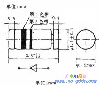
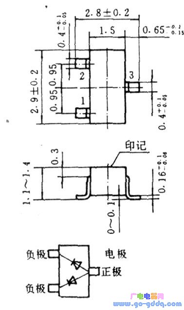
The diodes are divided into leadless cylindrical and sheet-shaped, and their external dimensions are shown in the above figure and the following figure.
The cylindrical diode has dimensions of φ1.5mm×3mm and φZ. It is available in 7mm x 5.2mm and is commonly used for Zener diodes, switching diodes and some general purpose diodes. The cylindrical diode can be made of both tantalum and silicon materials; its lead polarity 甩 ribbon indicates that a ribbon near the lead indicates that the lead is the negative terminal. The cylindrical diode consumes 0.5 to 1 W.
The chip diode is a plastic rectangular sheet, and its size is generally 3.8×1.5×11 (mm). FIG. 10 is a schematic diagram of a composite diode with three short leads.
Both of these diodes are available in tape and reel packaging.
2. Transistor
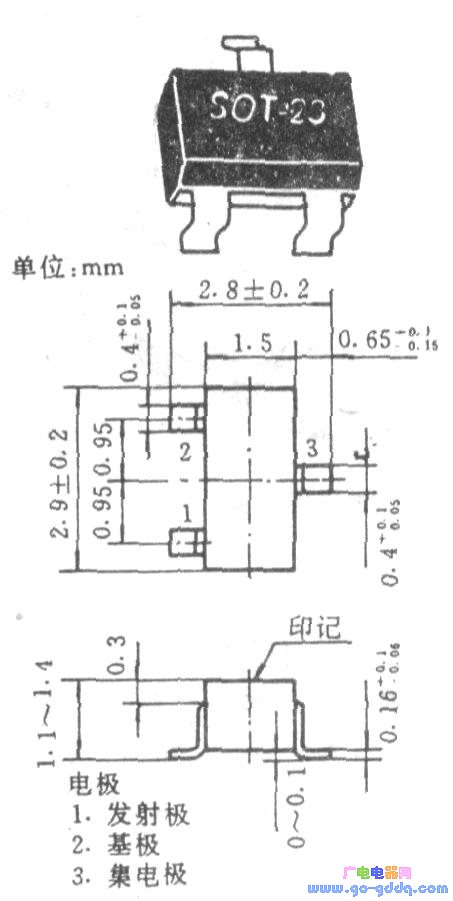
The ordinary triode adopts the outer structure as shown in the figure below. Ordinary triodes generally consume 150 to 300 mW of power, both of which are low-power silicon (or germanium) tubes.
Double-gate FETs and high-frequency transistors often use the outline structure shown in the following figure.
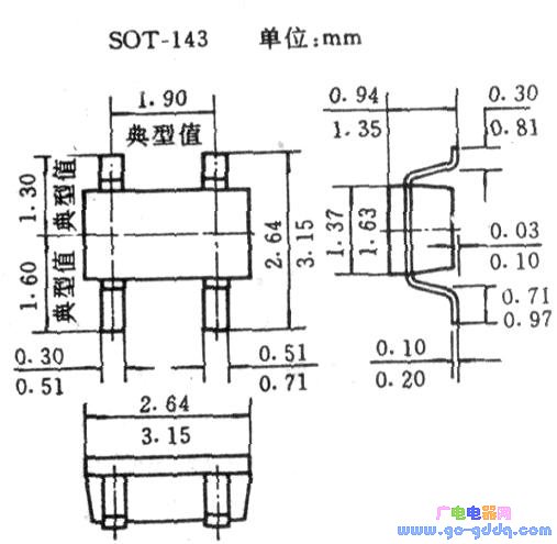
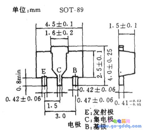
The high-powered high-frequency transistor adopts the outer structure as shown in the following figure, and its size is 4.5 × 2.5 × 1.5 (mm). The chip is attached to a larger piece of copper to increase heat dissipation. The power consumption of such a pipe is 300mW to 2w. Of course, there are also more powerful tubes, and the package shape is similar to that of a common high power tube.
3. The early products of integrated circuit surface mount integrated circuits were plastic-sealed structures with winged leads with pin pitches that were smaller than conventional. These products are available in SOP, SOJ small outline package circuits and QFP square flat package circuits. Since then, the chip carrier technology has been developed, and there have been PLCC plastic packaged lead chip carriers, LCCC leadless ceramic chip carriers, LDCC leaded ceramic chip carriers, COB onboard chips. In recent years, TAB loaded automatic welding products have been developed.
(1) SOP, SOJ small outline package circuit This technology was successfully developed by Philips in the Netherlands in the early 1970s. It is actually a variant of the dual in-line package circuit. The SOP is an "L" shaped lead, as shown in the figure below, and the SOJ is a "J" shaped lead.
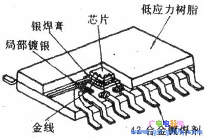
As shown below;
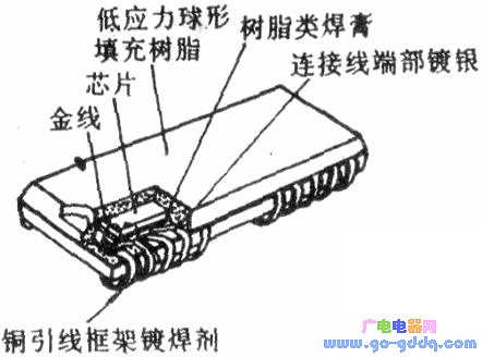
The figure below shows the outline of the two circuits.
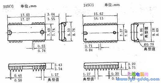
The characteristic of the SOP package circuit is that the leads are easy to solder, and the detection process is convenient, but the area occupied by the printed board is large. The SOJ package circuit occupies a small area of ​​the printed board, so it is currently used more widely. The pitch of the pins is 1.27mm, and the pitch is 1. Omm and 0.76mm.
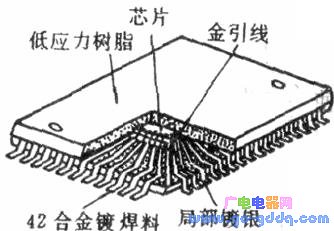
(2) QFP square flat package circuit This is a new type of package circuit developed and manufactured by some Japanese manufacturers for small pitch surface mount circuits. The structure is shown in the figure below.
The figure below shows the external dimensions of a QFP circuit.
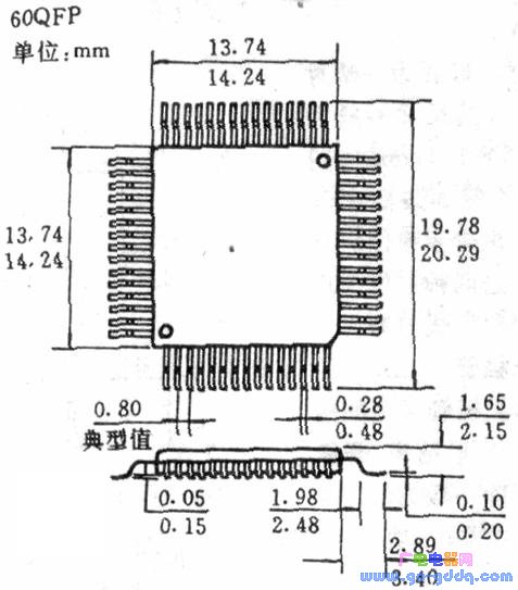
Due to the large number of leads (32-576 strips), the QFP package circuit has a large contact surface and thus has a high soldering strength. However, since the leads are too soft and the pitch is too small, it is difficult to install and solder.
QFP packaged circuits are available in square and rectangular packages with lead pitches of 0.3, 0.4, and 0.5 (mm). At present, a thin QFP (also known as TQFP) introduced by Hitachi has a lead pitch as small as 0.254 mm and a circuit thickness of only 1.2 mm.
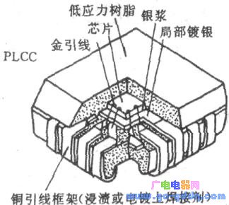
(3) PLCC plastic packaged lead chip carrier PLCC packaged lead chip carrier has short leads on its four sides bent to the bottom of the "J" shape, as shown in the figure above. Obviously, PLCC saves PCB area more than SOP and QFP. However, it is more difficult to detect the solder joints after soldering the circuit to the printed board, and it is more difficult to repair the solder joint. Such package circuits are often microcomputer central processing units and gate array circuits. At present, the corresponding clip-in board has been developed to solve the solder joint test problem. (4) COB onboard chips are commonly referred to as "soft" packages and "black glue" packages. It is to directly attach the IC chip to the printed board, wire bonding to achieve the connection with the printed board, and finally coating the package with black rubber. Such circuits are low in production cost and are mainly used in low-cost consumer electronic products such as electronic timepieces, game consoles, calculators, toys, electronic doorbells, and the like. These chips and leads are sealed on the printed board with black glue and are disposable installation circuits, making it impossible to replace them.
Of course, surface mount components, in addition to the above, there are also such as chip inductors, composite components, electromechanical components, sensitive components, etc., due to space limitations, this article will not be introduced one by one.
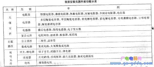
The above table and the following table for the classification of surface mount components.
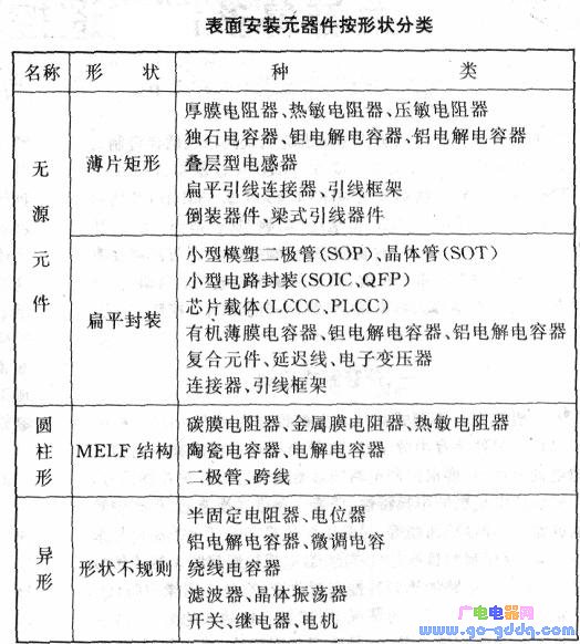
4. Replacement requirements for mounting semiconductor devices in the West
The following focuses on the repair and replacement methods and precautions under amateur conditions.
Generally speaking, when a surface mount diode, a triode, a FET, or a power tube of a whole machine (component) such as a TV tuner, a calculator, a game machine, or the like is damaged, since the internal space is large, the device of the conventional lead can be directly used. Lap soldering on damaged components on the printed board. When the lead distance is small, the lead should be cut as short as possible, and it is better to put on the insulating sleeve to avoid shorting the lead. The component leads should be tinned, and the soldering iron tip used for soldering should be sharpened. When welding, use a pair of tweezers to clamp the components. After the soldering iron is attached with a proper amount of tin, lick the rosin, and then quickly perform spot welding. The welding time is preferably within 3 seconds. When repairing an electrical device such as an electronic watch, a portable device, or a camera with a small space inside the machine, only the chip component is selected. At this point, it should be noted that the electrical parameters of the selected component should be consistent with or better than the damaged component (only components with low performance parameters can be selected with circuit approval). Some components are not well clamped with tweezers. You can use 502 glue (or epoxy resin, but increase the proportion of curing gel to facilitate quick drying), then stick a thin solder wire, hold a soldering iron, and hold the soldering iron. The leads are spot welded. In this case, the component leads may not be pre-tinned as long as the leads are of the correct polarity.
The operation of replacing an integrated circuit is much more complicated. Remove the damaged lc. A tin soldering iron should be used, and if there is an electric soldering iron, it is better. First remove the solder from all the leads. As long as the tin is sucked, the IC can be removed directly. For ICs that have been judged to be damaged, you can also cut all the leads with a knife, then use the soldering iron to absorb the solder joints, and finally clean the pads with alcohol, and carefully check the pads with a magnifying glass to confirm the solder joints. Then go to the next step to replace the work.
The IC to be replaced should be the same as the original IC model. If you use replacement parts, you should carefully check the replacement information, but it is best to use direct replacement parts (ie, function, lead, and shape are exactly the same). The rC lead should not be pre-tinned, otherwise it is easy to produce continuous welding. After putting 1C correctly, first fix the two leads with the soldering iron diagonally, then hold the solder wire, hold the soldering iron, and spot weld all the leads. During the spot welding process, the amount of solder wire supplied should be controlled, because there will be continuous soldering due to excessive soldering. During the operation, the wrist should wear the static elimination ring, and the electric iron should be grounded to avoid static damage to the circuit, especially in the dry environment. The method of self-made wrist anti-static ring is to cut the black conductive foam plastic for packaging integrated circuit into a 15cm long, 1~2cm wide plastic strip with a multi-strand copper wire inside, and the other end of the wire is connected to the power socket. When protecting the "ground" end, if there is no protection "ground", you should smash an iron of about 1 meter underground. It is extremely unsafe to replace the protected area with a water pipe or a heating pipe.
Electronic Cigarette,Largest E-Cig Oem,China E-Cig Oem,Vape Pen Oem,Vape Device Oem
Shenzhen MASON VAP Technology Co., Ltd. , https://www.cbdvapefactory.com