abstract
The thermal characteristics of the IC package are very important parameters for IC application and reliability. This paper describes in detail the main parameters of the thermal characteristics of the standard package: thermal resistance (ΘJA, ΘJC, ΘCA) and other parameters. In this paper, the development of thermal resistance related standards, physical meaning and measurement methods are introduced in detail, and some empirical methods of thermal calculation and thermal management in practical systems are proposed. It is hoped that electronic devices and system design engineers can understand the relevant principles and applications of thermal resistance values ​​to solve the overheating problems of devices and systems.
introduction
According to the continuous development of the Moore's theorem, the density of integrated circuits is getting higher and higher, and the size is getting smaller and smaller. All integrated circuits will generate heat during operation. The accumulation of heat will inevitably lead to an increase in the temperature of the semiconductor junction. As the junction temperature increases, the performance of the semiconductor components will decrease, and even the chip will be damaged. Therefore, each chip manufacturer will specify the maximum junction temperature of its semi-conductor device. In order to ensure that the junction temperature of the component is below the maximum allowable temperature, efficient heat dissipation from the IC itself to the surrounding environment via the package is critical. In the ordinary digital circuit, since the power consumption of the low-speed circuit is small, under normal heat dissipation conditions, the temperature rise of the chip is not too large, so the heat dissipation problem of the chip is not considered. In high-speed circuits, the power consumption of the chip is large, and the heat dissipation under natural conditions cannot guarantee that the junction temperature of the chip does not exceed the allowable operating temperature. Therefore, it is necessary to consider the heat dissipation problem of the chip so that the chip can work at a normal temperature. Within the scope.
1 thermal characteristics basis
Under normal conditions, heat transfer is carried out by conduction, convection, and radiation. Conduction is the transfer of heat from high temperature to low temperature through the contact of objects. The better the thermal conductivity, the better the thermal conductivity. Generally, the thermal conductivity of metal is the best; convection is the flow of heat away from the flow of objects, liquids and gases. The faster the flow rate, the more heat is removed; the radiation does not require a specific intermediate medium, and the heat is sent directly, and the effect is better in vacuum.

2 thermal resistance
The heat of the semiconductor device is mainly dissipated through three paths: the top of the package to the air, the bottom of the package to the board and the package leads to the board.
One of the most common and most important parameters in the heat dissipation of electronic devices is the Thermal Resistance. Thermal resistance is an important indicator of the thermal conductivity of a substance. In the case of integrated circuits, thermal resistance is a measure of the ability of a package to conduct the heat generated by the die to the board or the surrounding environment. The definition is as follows:
The thermal resistance value is generally indicated by ??, where Tj is the temperature of the chip Die surface (junction temperature), Tx is the temperature at which heat is conducted to a certain target point, and P is the input heating power. In electronic design, a voltage difference is generated if current flows through the resistor. Similarly, if the heat flows through the thermal resistance, a temperature difference will occur. A large thermal resistance means that heat is not easily conducted, so the temperature generated by the device is relatively high, and the thermal resistance can be used to judge and predict the heat generation of the device. Normally, the junction temperature of the chip increases, the life of the chip decreases, and the failure rate increases. The chip may be damaged when the temperature exceeds the rated maximum junction temperature given by the chip.

Figure 1. Schematic diagram of chip thermal resistance
ΘJA is the thermal resistance of the chip Die surface to the surrounding environment, the unit is °C/W. The surrounding environment is often seen as a hot "ground" point. ?? JA depends on IC package, board, airflow, radiation, and system characteristics, and the effects of radiation are usually negligible. ΘJA refers to the value of natural conditions (without ventilation). Since the measurements are tested under standard specifications, different results can be obtained for different substrate designs and environmental conditions, so this value can be used to compare the ease with which the package dissipates heat for qualitative comparison.
ΘJC is the thermal resistance of the chip Die surface to the package case, and the case can be regarded as a specific point on the outer surface of the package. ΘJC depends on the package material (lead frame, molding material, die bond material) and the specific package design (die thickness, exposed pad, internal thermal vias, thermal conductivity of the metal material used). For leaded packages, the reference point of the ΘJC on the housing is located on the 1 pin of the plastic housing. In a standard plastic package, the ΘJC is measured at 1 pin. This value is mainly used to evaluate the performance of the heat sink.
Note that ΘJC represents only the resistance of the heat dissipation path to the package surface, so ΘJC is always less than ΘJA. ΘJC indicates the thermal resistance of a specific heat dissipation path that conducts heat by conduction, while ΘJA indicates the thermal resistance of a heat dissipation path that conducts heat by conduction, convection, or radiation.
ΘCA refers to the thermal resistance from the chip package to the surrounding environment. ΘCA includes the thermal resistance of all heat dissipation paths from the outer surface of the package to the surrounding environment. According to the definition given above, we can know: ΘJA =ΘJC+ΘCA
ΘJB refers to the thermal resistance from the surface of the chip to the board. It quantifies the thermal path from the surface of the chip Die to the board and can be used to evaluate the heat transfer performance of the PCB. ΘJB includes thermal resistance from two aspects: the thermal resistance from the Die surface to the reference point at the bottom of the package, and the thermal resistance of the board through the bottom of the package. This value can be used to evaluate the heat transfer performance of the PCB.
From here, we can see that there are three main paths for heat transfer. First, the heat on the surface of the chip Die is conducted to the surface of the device through the Mold Compound and then radiated by convection heat/radiation. Second: Yes Chip Die surface to pad, then convective/radiative dispersion by printed circuit board connected to the pad. Third: The surface heat of the chip is transferred to the PCB through the Lead Frame for heat dissipation. Obviously the value of ΘJA is closely related to the external environment.
The definitions of Ψ and θ are similar, but the difference is that Ψ refers to most heat transfer conditions, and θ refers to total heat transfer. When the actual electronic system dissipates heat, the heat will be transmitted from the top and bottom of the package, and not necessarily from a single direction. Therefore, the definition of Ψ is in line with the measurement status of the actual system. ![]() JB is the thermal characteristic parameter of the chip Die surface to the board, the unit is °C/W, and the thermal characteristic parameters are different from the thermal resistance. Relative to thermal resistance
JB is the thermal characteristic parameter of the chip Die surface to the board, the unit is °C/W, and the thermal characteristic parameters are different from the thermal resistance. Relative to thermal resistance ![]() The direct single path is different when JB is measured.
The direct single path is different when JB is measured. ![]() The component power flux measured by JB is based on multiple thermal paths. Since the thermal path of these JBs includes thermal convection at the top of the package, it is more convenient for the user's application.
The component power flux measured by JB is based on multiple thermal paths. Since the thermal path of these JBs includes thermal convection at the top of the package, it is more convenient for the user's application.
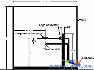
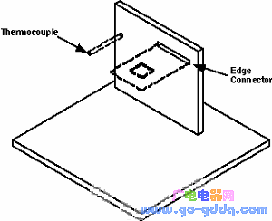
The measurement of the thermal resistance is given by the JESD51 standard. The structural configuration defined in JEDEC is not a typical system reflection in practical applications, but a standardized thermal analysis and thermal measurement method for consistency and standardization. This helps to compare thermal performance metrics for different package variations. The standard environment is to mount the device on a larger printed circuit board and place it in 1 cubic foot of still air. So the value in the description is actually a system level parameter.


Figure 2. Schematic diagram of JESD51 standard chip thermal resistance measurement environment
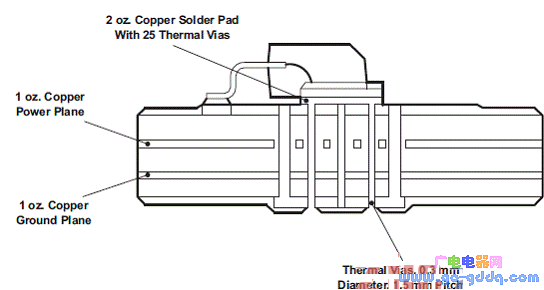
Take the TO263 example, which includes a standard JEDEC high-K board (2S2P) with a 1 ounce internal copper plane and ground plane. The package is soldered to a 2 ounce copper pad. This chassis is connected to the 1 ounce ground plane via a thermal via. The operating environment used in the computer model is shown in the side view of the figure below.

Figure 3. TO-263 thermal resistance model
JESD is a complete set of standards. Specific standards can be found on the relevant website.
JESD51: Methodology for the Thermal Measurement of Component PACkages (Single SEMIconductor
Device)
JESD51-1: Integrated Circuit Thermal Measurement Method - EleCTRical Test Method (Single Semiconductor Device)
JESD51-2: Integrated Circuit Thermal Test Method Environmental Conditions——Natural Convection (StillAir)
JESD51-3: Low Effective Thermal Conductivity Test Board for Leaded Surface Mount Packages
JESD51-4: Thermal Test Chip Guideline (Wire Bond Type Chip)
JESD51-5: Extension of Thermal Test Board Standards for Packages with Direct Thermal Attachment Mechanisms
JESD51-6: Integrated Circuit Thermal Test Method Environmental Conditions - Forced Convection
(Moving Air)
JESD51-7: High Effective Thermal Conductivity Test Board for Leaded Surface Mount Packages
JESD51-8: Integrated Circuit Thermal Test Method Environmental Conditions - Junction-to-Board
JESD51-9: Test Boards for Area Array Surface Mount Package Thermal Measurements
JESD51-10: Test Boards for Through-Hole Perimeter Leaded Package Thermal Measurements.
JEDEC51-12: Guidelines for Reporting and Using Electronic Package Thermal Information.
BAM Power Transmission Capacitors
BAM power transmission capacitors
RAM/RFM Induction Heating Capacitors,Water Pump Capacitor,Water Cooled Condense,Tank Capacitor
YANGZHOU POSITIONING TECH CO., LTD. , https://www.cnfudatech.com