Replacing the original EL backlight and CCFL backlight of the handheld device with LED backlight not only makes the circuit design simpler and easier, but also has higher external force resistance. Replacing the original CCFL backlight of LCD TVs with LED backlights is not only more environmentally friendly, but also displays more vivid and beautiful. LED lighting instead of white light, halogen light and other lighting, not only more bright and energy-saving, the use is also longer, and the lighting response is faster, can reduce the rear car collision rate when used in the vehicle lights.
Therefore, LEDs can only be used in the state of the electronic device in the past, to become the backlight of the liquid crystal display, and then extended to electronic lighting and public display, such as car lights, traffic lights, kanban message marquees, large-scale film and television Walls, even lighting in projectors, continue to extend their applications.
More importantly, the brightness efficiency of LEDs is the same as Moore'''s Law, which doubles every 24 months. In the past, white LEDs could only be used to replace incandescent and halogen lamps that consume too much power. That is, the luminous efficiency is within the level of 1030 lm/W. However, after the white LED breaks through 60 lm/W or even 100 lm/W, even fluorescent lamps and high-pressure gas discharge lamps are beginning to feel threatened.
Although LEDs continue to enhance brightness and luminous efficiency, in addition to the patented technologies such as the most fluorescent materials and mixed light, it will become an increasingly challenge for packaging, and it is a double challenge. On the one hand, packaging must be Let the LED have the maximum light extraction rate and the highest luminous flux to minimize the light loss, and also pay attention to the divergence angle of the light, the light uniformity, and the compatibility with the light guide plate.
On the other hand, the package must have the best heat dissipation of the LED, especially HB (high brightness) almost means HP (High Power, high power, high power), the current value of the LED is continuously increased, if not Good heat dissipation will not only reduce the brightness of the LED, but also shorten the life of the LED.
Therefore, the continuous pursuit of high-brightness LEDs, if the package technology used does not have the corresponding enhancement, then the high-brightness performance will be discounted. Therefore, this article will discuss more about the packaging technology of HB LEDs, including the discussion of optical communication. Also includes discussion on thermal conductivity.
Note 1: In general, HB LEDs refer to luminous efficiencies above 8 lm/W (8 lumens per watt).
Note 2: In general, HP LEDs use more than 1W (watts) of power, and the power consumption wattage is obtained by multiplying the forward voltage by the forward conduction current (Vf × If, f = forward).
Bare layer: "quantum well, multi-quantum well" enhances "light conversion efficiency"
Although this article is mainly about the enhancement of the luminous flux of the LED package, it is necessary to first explain the bare part of the deeper core. After all, the improvement of the bare crystal structure can also greatly increase the luminous flux.

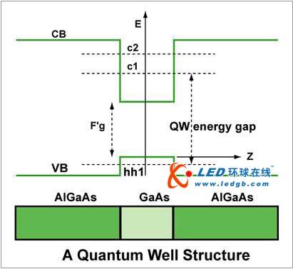
The first is to enhance the efficiency of light conversion, which is also the most fundamental way. Only 15% and 20% of the electricity used per watt of LED is converted into light energy, and the rest are converted into heat energy and dissipated (waste heat). The key to improving this conversion efficiency is on the pn junction. The pn junction is the main illuminating heat-emitting position of the LED. The structural design change through the pn junction can improve the conversion efficiency.
In this regard, at present, Quantum Well (QW) is often built on the pn junction to increase the proportion of electricity converted into light energy, and further efforts will be made toward more cuttings. Multiple Quantum Well (MQW) technology.
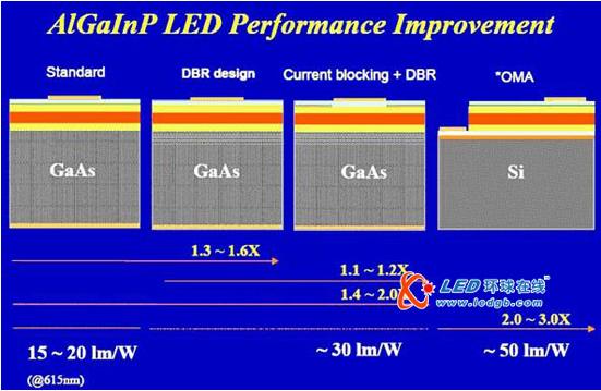
Bare layer: "Refueling and remodeling, light and light folding" to raise the "light efficiency"

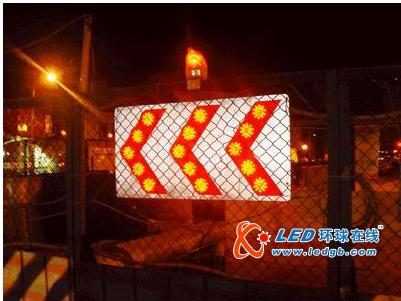
LEDs with improved brightness have already reached the application of the public in the public. This is the traffic direction indicator on the periphery of the domestic construction site, which is composed of HB LEDs.
Note 3: AlGaInP (aluminum gallium indium phosphide) is also called "quaternary luminescent material", which is a combination of four elements of Al, Ga, In, and P.
Note 4: In the general graphic structure explanation, the pn junction is also called "lighting layer, emitting layer or active layer, active region".
Note 5: In addition to reducing light coverage and increasing reflection, sometimes the intention to switch to different technologies is to circumvent patents that have been applied for by other companies.
