Summary
Recently, the LLC topology has been favored by power supply design engineers for its high efficiency and high power density. However, this soft switching topology requires more MOSFETs than any previous hard switching topology. Especially in the case of power start, dynamic load, overload, short circuit, etc. With its fast recovery body diodes, low Qg and Coss, CoolMOS can fully meet these requirements and greatly improve the reliability of the power system.
For a long time, improving the power density, efficiency and reliability of power systems has always been a major issue for researchers. Increasing the switching frequency of the power supply is one of the methods, but the increase of the frequency will affect the switching loss of the power device, so that the lifting frequency is not very effective for the hard switching topology, and the hard switching topology has reached its design bottleneck. . At this time, soft switching topologies, such as LLC topology, are sought after by design engineers for their unique characteristics. But... This topology puts new demands on power devices.
2. Features of the LLC circuit
The following features of the LLC topology make it widely used in a variety of switching power supplies:
1. LLC converters enable zero voltage switching over a wide load range.
2. The output can be adjusted with a wide range of input voltage and load changes, while the switching frequency changes relatively small.
3. Using frequency control, the duty ratio of the upper and lower tubes is 50%.
4. Reduce the voltage stress of the secondary synchronous rectifier MOSFET, you can use a lower voltage MOSFET to reduce costs.
5. No need for output inductors, which can further reduce system cost.
6. The use of lower voltage synchronous rectifier MOSFETs can further improve efficiency.
3. The basic structure and working principle of the LLC circuit
Typical circuit and operating waveforms of the LLC resonant converter are shown in Figures 1 and 2, respectively. The LLC converter shown in Figure 1 consists of two power MOSFETs (Q1 and Q2) with a duty cycle of 0.5; a resonant capacitor Cr, a center-tap transformer Tr with the same number of turns, an equivalent inductance Lr, and excitation. Inductor Lm, full-wave rectifier diodes D1 and D2 and output capacitor Co.
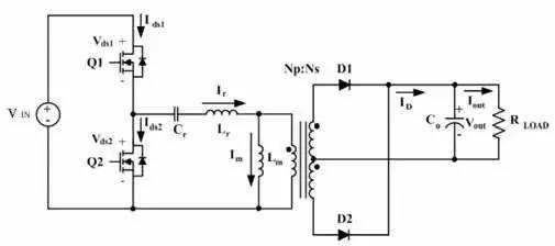
Figure 1 Typical circuit of a LLC resonant converter
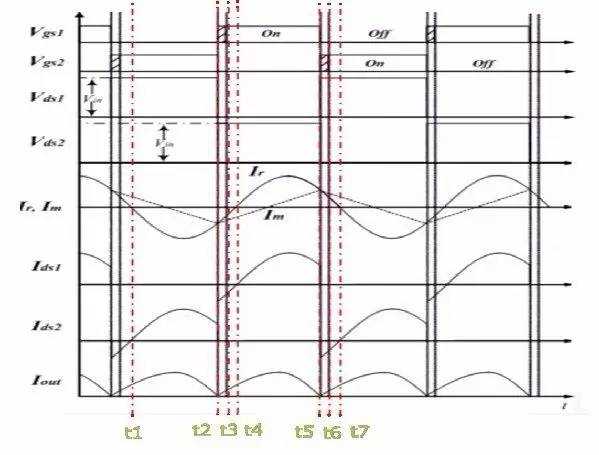
Figure 2 The operating waveform of the LLC resonant converter
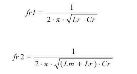
The LLC has two resonant frequencies, Cr, Lr determine the resonant frequency fr1; and Lm, Lr, Cr determine the resonant frequency fr2.
When the load of the system changes, the operating frequency of the system changes. When the load increases, the switching frequency of the MOSFET decreases. When the load decreases, the switching frequency increases.
3.1 LLC resonant converter operating timing
The steady state operation of the LLC converter is as follows.
1) [t1, t2]
Q1 turns off, Q2 turns on, inductor Lr and Cr resonate, secondary D1 turns off, D2 turns on, diode D1 is about twice the output voltage, and energy is converted from Cr, Lr to secondary. Until Q2 is turned off.
2) [t2, t3]
Q1 and Q2 are turned off at the same time. At this time, the dead time is at this time. At this time, the inductor Lr, Lm current charges the output capacitor of Q2, and discharges the output capacitor of Q1 until the voltage of Q2 output capacitor is equal to Vin.
Secondary D1 and D2 turn off Vd1 = Vd2 = 0, and the phase ends when Q1 is turned on.
3) [t3, t4]
Q1 turns on and Q2 turns off. D1 is turned on, D2 is turned off, and Vd2=2Vout
Cr and Lr resonate at fr1, at which point the current of Ls returns to Vin through Q1 until the current of Lr ends at zero phase.
4) [t4, t5]
Q1 is on, Q2 is off, D1 is on, D2 is off, Vd2=2Vout
Cr and Lr resonate at fr1, and the current of Lr flows back through Q1 to power ground. Energy is converted from input to secondary until Q1 turns off the phase ends
5) [t5, t6)
Q1, Q2 are turned off at the same time, D1, D2 are turned off, the primary current I (Lr+Lm) charges the Coss of Q1, and discharges Coss2 until the Coss voltage of Q2 is zero. At this point, the Q2 diode begins to conduct. The phase ends when Q2 is turned on.
6) [t6, t7]
Q1 is turned off, Q2 is turned on, D1 is turned off, D2 is turned on, Cr and Ls are resonant at frequency fr1, and Lr current is returned to ground via Q2. The phase ends when the Lr current is zero.
3.2 LLC resonant converter abnormal state analysis
The above description is that the LLC works in the resonant mode. Next, we analyze the operation of the LLC converter under start-up, short-circuit, and dynamic load.
3.2.1 Starting state analysis
Through the LLC simulation, we get the waveform shown in Figure 3. At the first switching cycle of the start, a short peak current Ids1 and Ids2 will appear simultaneously in the upper and lower tubes. Since the output capacitor Coss of the lower tube Q2 is charged when the MOSFET Q1 is turned on, the charging ends when Vds is high. The peak currents Ids1 and Ids2 are also generated by Vin charging the Q2 junction capacitance Coss through the MOSFET Q1.
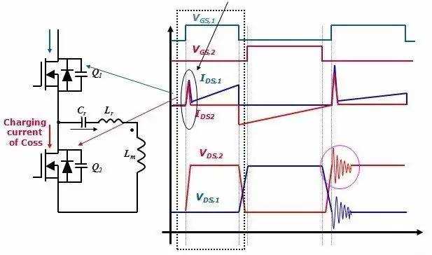
Figure 3 LLC Simulation Waveform
We focus on the second switching cycle as shown in Figure 4. We find that there is also a spike current similar to the first switching cycle, and the peak value will be higher, and the MOSFET Q2 Vds also has a very high dv. /dt peak voltage. So is this peak current still caused by Coss? Let's do further research.
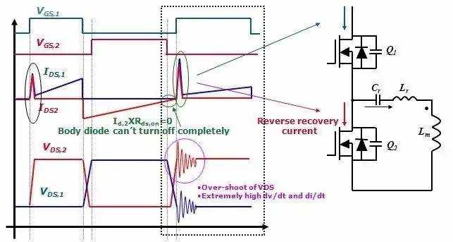
Figure 4 The second switching cycle waveform
Engineers who have a certain understanding of the MOSFET structure know that MOSFETs are different from IGBTs. In the MOSFET, there is actually a body diode parasitic. Like ordinary diodes, neutralization carriers are needed to reverse recovery during the turn-off process. The reverse voltage can be used to make this reverse recovery fast, and the energy required for reverse recovery is related to the charge Qrr of the diode. The reverse recovery of the body diode also requires a reverse of the body diode. Voltage. The voltage applied across the diode at start-up is Vd=Id2 x Ron. While Id2 is almost zero at start-up, the diode takes a long time to reverse recovery when Vd is low. If the dead time is not set enough, the high dv/dt shown in Figure 5 will directly trigger the BJT in the MOSFET to break through the MOSFET.
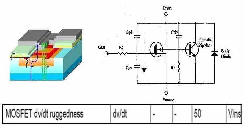
Figure 5
Through actual testing, we can repeat a similar waveform. The second switching cycle produces a peak current that is much higher than the first switching cycle, while the dv/dt is 118.4V/ns high when the MOSFET is turned on. The Vds voltage is more than the maximum value of 600V. The MOSFET is at risk when it is turned on.
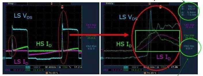
Figure 6
3.2.2 Abnormal state analysis
Below we continue to analyze the potential risks to the LLC topology when the load changes drastically.
The critical device MOSFET of the LLC circuit also faces challenges when the load changes drastically, such as short circuit, dynamic load and other conditions.
The LLC will typically go through the following three states when the load changes. We call it a hard turn-off, and in the right picture we can compare the difference in internal carrier variations between the traditional MOSFET and CoolMOS in these three timings, and the risk to the MOSFET.
(Click on the image to see a larger image)
Timing 1, Q2 zero voltage is turned on, reverse current flows through the MOSFET and the body diode, at this time the secondary diode D2 is turned on, and D1 is off.
- The conventional MOSFET current flows through the channel region, thereby reducing the number of holes
-CoolMOS is the same as the traditional MOSFET, the electron current flows through the channel, and the hole is reduced. The difference is that the P-well structure of CoolMOS is established at this time.

Timing 2, Q1 and Q2 are turned off at the same time, and the reverse current flows through the body diode of MOSFET Q2.
The internal electron and hole paths and flow directions are not much different for conventional MOSFETs and CoolMOS when Q1 and Q2 are turned off.

Timing 3, Q1 starts to turn on at this time. Due to the change of load, the body diode of MOSFET Q2 takes a long time to reverse recovery. When the reverse recovery of the diode is not completed, the MOSFET Q2 is hard-off. At this time, Q1 is turned on, and the voltage applied to the Q2 body diode forms a large current in the diode, which triggers the BJT inside the MOSFET to cause an avalanche.
- The conventional MOSFET is now pulled out by the carrier, at which time the electrons are concentrated around the PN junction, and the hole current is congested at the edge of the PN junction.
-CoolMOS's electron current and hole current are all in the same way. At this time, the hole current flows in the established P well structure, and there is no electron congestion.
In summary, when the LLC circuit is overloaded, short-circuited, dynamically loaded, etc., once the diode cannot be reversely recovered in the dead time, the large composite current generated will trigger the BJT inside the MOSFET to disable the MOSFET.
Some CoolMOS adopts the Super Juction structure. In the state where the MOSFET is hard-off, the carriers will recombine along the vertically constructed P well, and there is basically no lateral current, which greatly reduces the chance of triggering the BJT.
4. How to implement ZVS more easily
From the above analysis, it can be seen that increasing the dead time of the MOSFET can provide sufficient diode reverse recovery time while reducing the risk of high dv/dt, di/dt on the LLC circuit. But is it the only option to increase dead time? Below we further analyze how to reduce the risk to improve system efficiency.
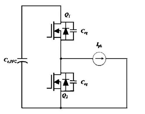
Figure 7
For the LLC circuit, the initial current for the dead time is

And LLC can achieve ZVS must meet
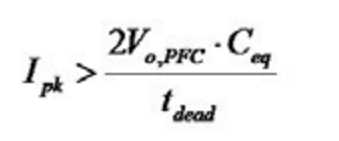
And the minimum magnetizing inductance is

According to the above three equations, we can implement LLC to implement ZVS in the following three ways.
First, increase Ipk.
Second, increase the dead time.
Third, reduce the equivalent capacitance Ceq, which is Coss.
From the above several conditions, we are not difficult to analyze. Increasing the Ipk will increase the inductor size and cost. Increasing the dead time will reduce the voltage during normal operation. The best choice is to reduce the Coss, because the reduction does not require any adjustment to the circuit, only a Coss is required. A small MOSFET can be used.
5. in conclusion
The LLC topology is widely used in a variety of switching power supplies, and this topology raises efficiency while also placing new demands on MOSFETs. Unlike the hard-switching topology, the soft-switching LLC resonant topology not only requires MOSFET's on-resistance (conduction loss), Qg (switching loss), but also how to effectively achieve soft switching, how to reduce the failure rate and improve System reliability and lower system cost have higher requirements. CoolMOS, with fast body diodes, low Coss, and some breakdown voltages up to 650V, makes the LLC topology switching power supply more efficient and reliable.
ZGAR bar Disposable
ZGAR electronic cigarette uses high-tech R&D, food grade disposable pod device and high-quality raw material. All package designs are Original IP. Our designer team is from Hong Kong. We have very high requirements for product quality, flavors taste and packaging design. The E-liquid is imported, materials are food grade, and assembly plant is medical-grade dust-free workshops.
Our products include disposable e-cigarettes, rechargeable e-cigarettes, rechargreable disposable vape pen, and various of flavors of cigarette cartridges. From 600puffs to 5000puffs, ZGAR bar Disposable offer high-tech R&D, E-cigarette improves battery capacity, We offer various of flavors and support customization. And printing designs can be customized. We have our own professional team and competitive quotations for any OEM or ODM works.
We supply OEM rechargeable disposable vape pen,OEM disposable electronic cigarette,ODM disposable vape pen,ODM disposable electronic cigarette,OEM/ODM vape pen e-cigarette,OEM/ODM atomizer device.


Disposable E-cigarette, ODM disposable electronic cigarette, vape pen atomizer , Device E-cig, OEM disposable electronic cigarette
Shenzhen WeiKa Technology Co.,Ltd. , https://www.zgarpods.com
