The converter (RF converter) that can directly synthesize signals in the radio frequency range has matured, and conventional radio design will change accordingly. Due to the ability to digitize and synthesize instantaneous signal bandwidths of up to 2 GHz to 3 GHz, RF converters can now fulfill the promise of providing true broadband radio. Radio designers can greatly simplify hardware design and support software reconfigurability. This is impossible for conventional radio design.
In today's article, we will discuss how advancements in RF converter technology make new data acquisition systems and broadband radios possible, and discuss the feasibility of software configuration.
Every radio designer has to face such a design trade-off, that is, the need to weigh performance and power consumption within the signal bandwidth. How radio designers meet this constraint determines the size and weight of the radio, and fundamentally affects the location of the radio, including buildings, towers, poles, underground vehicles, packages, pockets, ears or glasses. Each radio location has an amount of available power commensurate with its location. For example, the power available on a building or tower is likely to be higher than that provided by a smartphone in your pocket or a Bluetooth headset in your ear. In all cases, there is a basic fact: the less power the radio requires, and the greater the throughput per unit power can support, the smaller the radio size and the lighter the weight. This fact has a huge impact and has been the driving force behind many innovations in the communications electronics industry for many years.
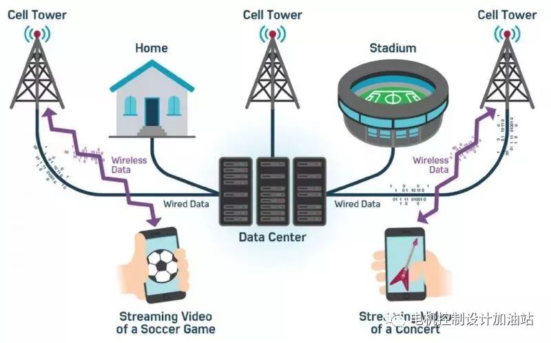
Figure 1. The RF converter supports broadband radio to provide services that require large amounts of data, such as video streaming and games.
Semiconductor companies integrate more functions and higher performance into devices of the same or smaller size, and devices using such devices can achieve smaller, more functions or lighter (in some cases all three can be Fulfilled) promises. The smaller, lighter, and more functions the device is, the better, so that the device can be placed where it could not be placed due to other constraints. For example, a building was originally needed, but now the equipment can be placed on a tower due to the reduced footprint; the radio unit that was originally placed on the tower can be reduced to a unit on a wire pole if the weight is light enough; originally because Units that are heavier and need to be carried by a vehicle can now be placed in a backpack.
Today’s environment is full of traditional devices that need to be placed on buildings, towers, pillars, and vehicles. Because of the need for people all over the world to interconnect with each other, engineers used the devices available at the time to design equipment to meet the challenges, and this has resulted in the ubiquitous environment in which we communicate today. We can make calls, send messages, instant messaging, transfer photos, download, upload and browse through a variety of different networks (including mobile networks, wireless local area networks, ad hoc short-range wireless networks, etc.) anytime and anywhere. All of these are connected to a broadband wired network, and the data is transmitted by RF cables and finally transmitted by optical fibers.
Enhanced video experience
A number of studies have shown that the demand for data is expected to continue to grow in the next ten years. The driving force is the seemingly endless demand for more data-rich content, which requires wider bandwidth. For example, cable television and fiber-to-the-home operators continue to compete in home broadband services by providing higher-speed connections and more high-definition TV channels. Ultra-high-definition (UHD or 4k definition) TVs require more than twice the capacity of high-definition TVs, and the channel bandwidth requirements exceed the bandwidth used today.
In addition, immersive videos including virtual reality (VR), games with multiple degrees of freedom and 3D effects (180° or panoramic vision, etc.) all use 4k ultra-high-definition TVs, and each user requires up to 1 Gb of bandwidth. This goes far beyond the already demanding requirements of simple 4k UHD TV broadcasting and streaming. Online games require the network to provide symmetrical data bandwidth, because the delay time is critical, which promotes the development of wider bandwidth uplink transmission capabilities. This demand for wider uplink capabilities in turn prompts equipment manufacturers to upgrade their designs to achieve symmetrical wide bandwidth transmission.
The powerful functions of today's RF converters are critical to the advancement of the transmission of such rich video content. Must be able to provide a large dynamic signal output, while requiring excellent spurious performance to support the use of higher order modulation schemes such as 256-QAM, 1024-QAM and 4k-QAM. The installed coaxial cable equipment and distribution amplifiers have a limited bandwidth of 1.2 GHz to 1.7 GHz. In order to improve the spectral efficiency of each channel, the above-mentioned higher-order modulation methods must be used. The higher performance of front-end transmission equipment can extend the service life of the installed equipment group, ease capital budget constraints, and support a longer window for multiple service operators (MSOs) to upgrade their equipment and transmission systems.
Multi-band, multi-mode test
With more and more integrated functions, today's smart phones are far from traditional mobile phones. Many functions have radios associated with them, so there may be five to seven or more frequency bands in current mobile devices. When producing smart phones, each radio must be tested, which brings new challenges to manufacturers of multi-mode communication testers. Although the amount of testing increases with the increase in the number of radios, rapid testing is still required to reduce the cost of testing. Considering the size and cost of the tester, it becomes impractical to build different radio hardware for each radio in a mobile device. As more frequency bands are opened or proposed for mobile services, the challenge of testing more and more radios in mobile devices is increasing.
RF converters can meet this challenge well. Whether it is a transmitter or a receiver, RF converters can provide flexibility that conventional radios cannot achieve. Broadband RF converters can simultaneously capture and directly synthesize signals in each frequency band, thereby supporting simultaneous testing of multiple radios in mobile devices. Using the channel selector built in RF DAC and RF ADC, multiple radio signals can be efficiently processed in the converter. For example, Figure 2 shows that each RF DAC has 3 sub-channel processing units, which can combine the signals of three different frequency bands, and then use the digitally controlled oscillator (NCO) for digital up-conversion, and then convert the RF DAC into an RF signal .
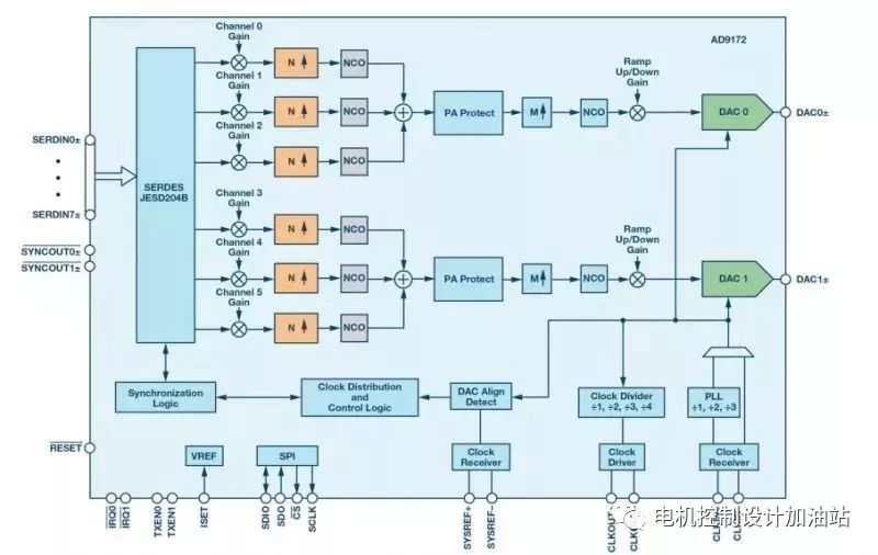
Figure 2. Example of RF DAC with channel selector
In other market areas, such as test equipment for the aerospace and defense markets, there is an increasing demand for broadband test solutions for pulse radar and military communications. Due to the large number and types of radar, electronic intelligence, electronic warfare equipment, and communication equipment that need to be tested, test equipment manufacturers must create a flexible instrument with a rich combination of features. For example, an arbitrary waveform generator must be able to create a variety of signals, including linear frequency modulated pulse signals, phase coherent signals, and modulated signals of various output frequencies and bandwidths. The measurement equipment must be equally powerful in order to receive these signals when testing exciters or transmitters. The RF converter supports direct RF synthesis and measurement at RF frequencies, which can serve such applications well. In some cases, this can eliminate the need for up-conversion or down-conversion, while in other cases, reduce the number of frequency conversions. The hardware is simplified, and the size, weight, and power consumption requirements are reduced. Adding digital features such as channel selectors, interpolators, NCOs, and synthesizers can realize high-efficiency signal processing on dedicated low-power CMOS technology.
Software defined radio
RF converter is one of the key factors of software-defined radio. The RF converter can directly synthesize and capture radio frequencies within a few GHz bandwidth, and realize the up-conversion or down-conversion function digitally, so that the entire up-conversion or down-conversion stage is no longer needed, and the radio architecture is simplified. Remove the analog frequency conversion stage and related mixers, LO synthesizers, and filters, which can reduce the size, weight and power consumption (SWaP) of the radio, so that the radio can adapt to more application scenarios and can be powered by a smaller power supply . This technology makes the radio small and light enough to be handheld, vehicle-mounted, or installed in various airborne assets such as airplanes, helicopters, and unmanned aerial vehicles (UAV).
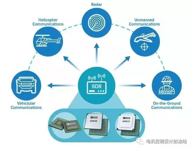
Figure 3. Software-defined radio driven by an RF converter supports cross-platform interconnection communications
In addition to achieving better cross-platform communication, radio hardware built with RF converters has the potential to support multiple functions, multiple modes, and multiple frequency bands. RF converters can now reach lower radar frequency bands, and will reach higher frequency bands in the near future, so the concept that a single device can be used as both a radar and a tactical communication link is expected to become a reality. Such a device has obvious advantages in terms of on-site maintenance, upgrades, procurement procedures and costs.
The ability to directly synthesize and capture radar frequencies makes RF converters very suitable for phased array radar systems. Direct RF converter synthesis and capture can reduce a lot of conventional radio hardware, making a single signal chain smaller and lighter. In this way, many of these radios can be integrated into a smaller space. Suitable for shipborne arrays or ground phased arrays, as well as smaller arrays and units for signal intelligence operations, can achieve smaller SWaP.
The technology behind the RF converter
One of the key technological advancements for the success of RF converters is the continuous scaling of fine-line CMOS processes. As the gate length and feature size of basic CMOS transistors become smaller, digital gate circuits become faster, smaller, and consume less power. This allows an RF converter with reasonable power consumption and area to integrate a large number of digital signal processing functions on the chip. Accommodating digital channel selectors, modulators, and software programmable filters are very important for building efficient and flexible radios. This more efficient DSP also opens the door for using digital processing to help correct analog defects in the converter. In terms of simulation, each new node provides faster transistors with better matching performance per unit area. These improvements are critical to the realization of faster high-precision converters.
It is not enough to rely on process technology progress alone, and there are some important architectural improvements that make RF converters possible. The preferred architecture of the RF DAC is the current steering DAC architecture. The performance of this type of DAC depends on the matching of the current sources constituting the DAC. The uncalibrated current source matching is proportional to the square root of the current source area7. The matching of unit area improves with the upgrade of technology nodes.
However, for high-resolution converters, even the most advanced nodes and the random mismatch is low enough, the current source will be very large. This kind of large current source will make the converter larger, and worse, the parasitic capacitance of the large current source will degrade the high frequency performance of the DAC. A more attractive solution is to calibrate a smaller current source to achieve the required level of matching. This can significantly reduce the additional parasitic effects from the current source and achieve the required linearity performance without compromising high-frequency performance. If performed correctly, this calibration can remain highly stable over the entire temperature range, and the calibration can be completed in one go. The stable one-time calibration means that there is no need to periodically run the calibration in the background, thereby saving operating power consumption and reducing the problem of spurious products caused by the background running calibration.
There is also an architecture choice that helps ultra-high-speed converters achieve performance targets, and that is the switch architecture choice for guiding the DAC current. The traditional double-switch structure (Figure 4) has several disadvantages when operating at very high speeds9,10. The data driven to the dual switch can remain unchanged for one to multiple clock cycles, so the setup time of the tail node depends on the data. If the clock rate is slow enough so that this node can be established within one clock cycle, then this is not a problem. However, at very high rates, this node cannot be fully established within one clock cycle, and depending on the setup time of the data will cause the DAC output to be distorted.
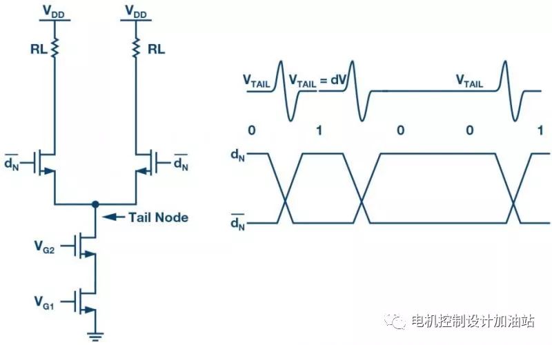
Figure 4. Example of a dual-switch DAC unit.
If you use a four-way switch (Figure 5), the data signals will all return to zero. This causes the tail node voltage to be independent of the data input, thereby alleviating the above-mentioned problems. The four-way switch also allows the DAC data to be updated on both edges of the clock. Using this feature can effectively double the DAC sampling rate without the need to double the clock frequency.
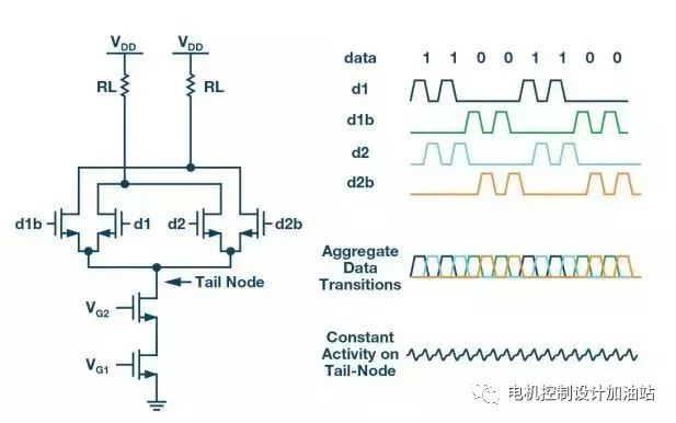
Figure 5. Example of a four-switch DAC unit
Using a well-designed current source calibration algorithm and four-switch current steering unit, combined with today's fine-line CMOS technology, a high-speed sampling DAC with excellent dynamic range can be designed. In this way, high-quality signals can be synthesized in a wide frequency range. When this wideband DAC is combined with an auxiliary DSP, it becomes a very flexible high-performance radio transmitter that can be configured to provide signals for all the different applications mentioned earlier in this article.
Future radio
Today's RF converters have led to fundamental changes in radio architecture design, and in the future, it will cause even greater changes. With the continuous advancement of process technology and the further optimization of RF converter design, the impact of RF converters on radio power consumption and size will continue to shrink. These technological advances are coming at the right time and have strongly promoted a new generation of radios, such as emerging 5G wireless base station applications (such as massive MIMO), and large-scale phased array radar and beamforming applications.
Deep sub-micron lithography technology will enable more digital circuits to be placed on the RF converter chip to integrate key functions that require a lot of calculations, such as digital predistortion (DPD) 13 and peak clipping (CFR) algorithms, etc., which will help To improve the efficiency of the power amplifier and significantly reduce the overall power consumption of the system. This integration will reduce the pressure on high-energy FPGA logic and transfer related functions to dedicated logic with lower power consumption. Other possibilities include integrating RF converters and their digital engines with RF, microwave, or millimeter wave analog devices to further reduce size and simplify radio design, and provide a system-level approach to radio design from bits to antennas. Thanks to the RF converter, various opportunities burst out.
RF converters are the technology that helps the world surpass all possibilities.
Based on ergonomic design principles. Raise the height of the display screen and stretch the distance between the eyes and the screen, so that notebook users will no longer be troubled by sub-health occupational diseases such as cervical pain and visual fatigue caused by long-term use of the notebook, and restore the normal state of easy office work.
Shenzhen Chengrong Technology Co.ltd is a high-quality enterprise specializing in metal stamping and CNC production for 12 years. The company mainly aims at the R&D, production and sales of Notebook Laptop Stands and Mobile Phone Stands. From the mold design and processing to machining and product surface oxidation, spraying treatment etc ,integration can fully meet the various processing needs of customers. Have a complete and scientific quality management system, strength and product quality are recognized and trusted by the industry, to meet changing economic and social needs .

Portable Laptop Stand Foldable,Lightweight Portable Laptop Stand,Portable Laptop Computer Stand,Portable Laptop Stand for Travel
Shenzhen ChengRong Technology Co.,Ltd. , https://www.dglaptopstandsupplier.com