introduction
Energy-saving and environmental protection technology is the focus of the current world. In the liquid crystal display module, the power consumption of the backlight can account for more than 50% of the total power consumption. Especially in portable devices such as mobile phones, PDAs, and MP3s that are displayed below 10 inches, battery power is basically used, and the power consumption problem is particularly prominent. In order to effectively reduce the brightness of the backlight of the liquid crystal display to achieve the purpose of power saving, this paper implements a backlight dimming method based on histogram transformation on the ARM development platform. Experiments show that the proposed method has a distortion of 5%. In the case of the backlight can save about 35%.
1 backlight dimming solution
Taking the TFT liquid crystal panel structure as an example, including a backlight, a polarizer, a liquid crystal array, a color filter and the like, the display image perceived by the human eye is a comprehensive effect of the above various parts. Assume that the backlight brightness is normalized and set to b (the real number in the [0,1] interval), 0 corresponds to the backlight off condition, and 1 corresponds to the maximum brightness of the backlight. If the light source is an LED, the adjustment of b may include current pulse width modulation, current amplitude adjustment, and the like.
Suppose the image is discussed as an 8-bit grayscale image. f(x, y) represents the grayscale value of a point (x, y) in the image, and x and y are the coordinates of the point. Then, the liquid crystal transmittance at the position of the point can be expressed as:
t (x,y)=f(x,y)/255 (1)
The brightness L(x, y) that can be observed by the image point is a combined effect of backlight illumination and liquid crystal transmittance, and can be expressed as an approximately linear combination of backlight luminance b and liquid crystal transmittance t (x, y):
L(x,y) =b·t (x,y) =b·f(x,y)/255 (2)
According to the requirements of visual light efficiency consistency, it is necessary to find a way to make the pixel gray value increase as much as possible (to compensate for the backlight b becoming smaller). In order to achieve this goal, the paper first limits the gray value range of the image to a certain interval, and then stretches the histogram to achieve the increase of the pixel gray value. The image histogram is cropped by the thresholds fgl and fgh so that some points in the image are clamped to fgl and fgh, the grayscale interval of the image is limited to [fgl, fgh], and the backlight dimming problem is converted to this histogram. How the cropped image should be adjusted so that its backlight can minimize brightness.
Obviously, for fixed distortion, fgl and fgh can have multiple values, and the value should be in the formula (3):
Min (fgh- fgl ) (3)
The purpose of this processing is to limit the grayscale interval of the image to a minimum range.
After the formula (3) is realized, the next step is to linearly move the histogram, so that the gray scale is shifted to the dark region by the whole fgl. Thus the image gray region is compressed by the original distribution in the interval [0, 255] at [0, fgh - fgl] interval.
Assuming that the backlight is dark, the image should be grayscale stretched to compensate for the brightness loss caused by the backlight. If the linear stretching method is adopted, it is obvious that the maximum multiple of stretching is 255/(fgh-fgl). At this time, the pixel gray level is not saturated, and the backlight brightness can be reduced from 1 to (fgh-fgl)/255. According to the formula (2) ), the processed image has the same visual effect before and after backlight adjustment.
2 hardware and software implementation
This experiment uses the mini2440 development board for verification. The mini2440 is a low-cost and practical ARM9 development board. The processor is Samsung S3C2440 (ARM920T, the highest frequency can reach 532MHz). The LCD screen supports black and white, 4 levels of gray, 16 levels of gray, 256 colors, 4,096 colors of STN liquid crystal display, the size is from 3.5 to 12.1in, the screen resolution can reach 1,024 × 768 pixels, the experiment uses 3.5in LED backlight TFT LCD screen.
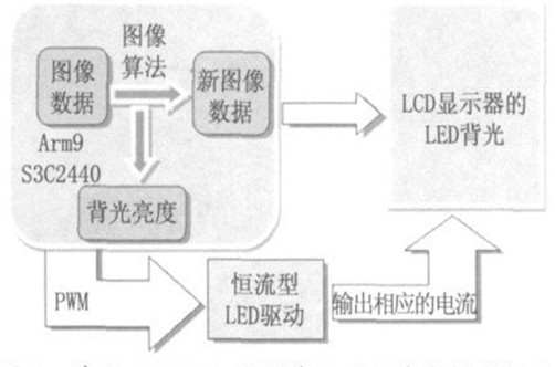
In the experiment, the gray value of the image is calculated according to the image algorithm, and the histogram of the displayed image is cropped to be limited to a certain range, and then the histogram is stretched, and then calculated by the calculation formula (fgh-fgl)/255. The display brightness of the backlight is controlled, and the duty ratio of the backlight pulse width modulation output pulse is controlled to realize the brightness adjustment of the backlight LED. The hardware block diagram is shown in Figure 1.

2.1 LED backlight drive design
The design adopts constant current LED driver, the output current is stable, the brightness of the backlight LED is constant, the output current is determined by changing the related peripheral resistance, and the switch control function with high sensitivity can realize the LED control by PWM. Brightness.
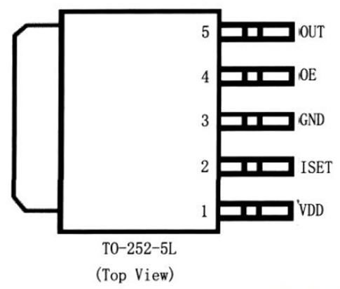
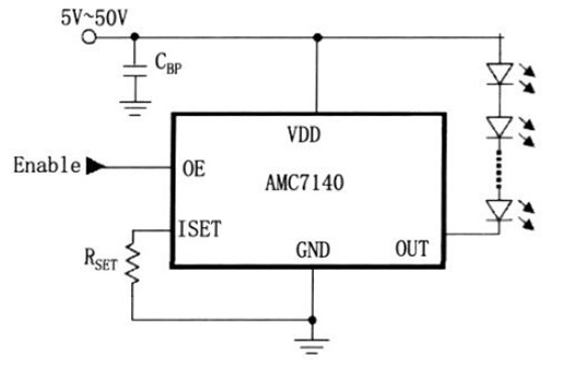
The AMC7140 is a high-power LED constant current driver IC with a wide voltage input DC range of 5~50V and an output current of up to 700mA. It is suitable for driving 1W, 3W, 5W LED lamps, TO-252-5L package with PWM CONTROL terminal ( OE pin). Figure 2 shows the pin diagram of the AMC7140, where pin 1 is the power supply input and pin 2 is the control terminal for the output current. The current is controlled by a high-precision resistor Rset ground. Current Iset=1.2V/ Rset, output current Iout=500×Iset; pin 3 is grounded; pin 4 is the PWM control terminal, active high; pin 5 is the output. The application circuit of the AMC7140 is shown in Figure 3.


2.2 Implementation of PWM Control Based on S3C2440
The S3C2440 has five 16-bit timers. Timers 0, 1, 2, and 3 have pulse width modulation (PWM); Timer 4 is an internal timer with no output pins; Timer 0 has a dead-time generator, which is commonly used in high-current devices; 1, 1 share an 8-bit pre-pulse divider, and timers 2, 3, and 4 share the other. Each timer has a clock divider that produces five divided signals (1/2, 1/4, 1/8, 1/16, and TCLK). Each timer module takes its own clock signal from its own clock divider, which takes the clock from the corresponding 8-bit pre-pulse divider. This 8-bit pre-pulse divider is programmable and divides the PCLK based on the values ​​in the TCFG0 and TCFG1 registers. After the timer is enabled, the initial value in the timer count buffer register (TCNTBn) is loaded into the down counter, and the initial value in the timer compare buffer register (TCMPBn) is loaded into the compare register for decrementing. The values ​​of the counters are compared. This double-buffering feature of TCNTBn and TCMPBn allows the timer to output a more stable signal when the frequency and duty cycle change. Each timer has its own clock-driven 16-bit down counter. When the counter is decremented to 0, a timer interrupt request is generated to notify the CPU that the timer operation is complete and the timer count buffer register value is automatically loaded again. Go to the down counter to continue the next operation. However, if the enable bit of timer TCONn is cleared in normal mode, the value of TCNTBn will no longer be loaded into the counter. The value of TCNTBn is often used for PWM. When the value of the down counter is equal to the value of the compare register, the timer control logic changes the output. Level, therefore, the compare register determines the on and off of the PWM output.
Set a timer, first initialize TCNTBn and TCMPBn, when initializing the timer, mainly set the following registers (take timer 0 as an example):
Timer output clock frequency = PCLK / (prescaler value + 1) / (divider value)
TCFG0 register setting: TCFG0=99; //prescaler value=“99â€
TCFG1 register setting: TCFG1=0x03; //divider value=“1/16â€
Thus, when PCLK = 400M, the timer output frequency is 6.25M.
The initial settings of the timer include:
TCNTB0 register setting: TCNTB0=62500; / / load initial value 1s interrupt once
TCMPB0 register setting: TCMPB0=rTCNTB0>1; //50%
Then you can start the timer, you must manually load it for the first time: TCON=1<1;
After loading, change to autoload and start the timer: TCON=0x09.
2.3 Image algorithm design based on S3C2440
The S3C2440 integrates an LCD controller to transfer image data to the LCD and provide necessary control signals such as VFRAME, VLINE, VCLK, VM, etc. It can support STNLCD and TFTLCD.mini2440 adopts 3.5in (resolution is 240×) 320 pixels) TFT LCD screen, configured in the usual 16BPP (5:6:5) mode. To display an image, simply write the pixel data (R(5):G(6):B(5)) to LCD_BUFFER, and the LCD controller will automatically read the data to the TFTLCD display via DMA.
The image algorithm is based on the image histogram for data transformation. Therefore, the subroutine should be written first and the gray histogram of the displayed image should be calculated first. The algorithm is as follows (where bmp is the original grayscale image and bmp_2 is the grayscale value). Array):
For( y = 0; y < 320; y++ )
{for(x = 0; x < 240; x++)
{bmp_2 [bmp[p]] ++;
p = p + 1;
}
}
Assuming a distortion of 5%, the number of pixels to be transformed is 240×320×5%=3,840 points. Then, according to the above algorithm principle, the point-by-point calculation method is used to calculate fgl from grayscale 0. (fgh-fgl), and finally find min(fgh - fgl).
In the next step, the histogram is linearly moved, so that the gray scale is shifted to the dark region by the whole fgl, so that the image gray region is compressed in the [0, fgh-fgl] interval by the original distribution in the [0, 255] interval. The image should then be grayscale stretched to compensate for the loss of brightness caused by the backlight. If the linear stretching method is adopted, it is obvious that the stretching is the most