LED display screen is a modern flat display screen composed of LED dot matrix module or pixel unit. It has the advantages of high luminous efficiency, long service life, large viewing angle range, rich color and strong adaptability to indoor and outdoor environments. The current LED display control system mostly uses ARM processor to complete the function of the whole system. This control system has great limitations in data processing speed and affects the continuity of display effect. Based on the analysis of the structure characteristics of STM32 microprocessor bus, the control system scheme of STM32+FPGA is proposed. This scheme fully utilizes the flexible memory control technology of STM32 microprocessor and the flexibility of programmable logic device. Sex, which improves the speed of system data processing, and simplifies the circuit structure and facilitates debugging.
1. System overall design
The system structure block diagram is shown in Figure 1.
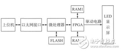
Figure 1 System block diagram
The system adopts the new generation 32bit RISC processor STM32 as the main control chip, transmits data through Ethernet, uses FLASH as the storage module, and completes the high-speed scanning and refreshing of the LED display by the FPGA. When the system works, the upper computer is used to edit the display information, and the display information is transmitted to the microprocessor through the Ethernet interface. The microprocessor receives the data information and writes it to the FLASH memory. During display, the microprocessor reads the data in the FLASH, and sends the data to the FPGA in parallel through the bus. After the FPGA processes the data, it transmits the data to the LED display.
2, system hardware design
This system selects ST's new 32-bit microprocessor STM32F103ZET6 as the main control chip. STM32F103ZET6 uses the ARMCORtex-M3 core with advanced architecture. Its flexible static memory controller makes it easy to connect with many memories and peripherals. At the same time, the STM32 has a large number of on-chip peripherals, which simplifies the design of the peripheral circuits of the system.
2.1, FLASH memory circuit design
FLASH uses Samsung's K9F1G16U0M, which is a NAND-type FLASH with a storage capacity of 64M16 bits and a working voltage of 3.3V. The connection between STM32F103ZET6 and K9F1G16U0M in the system is shown in Figure 2. IO0~IO7 of FLASH memory are connected with the lower 8 bits of FMSC data bus, STM32 processor accesses memory through FSMC; chip select signal nCE of FLASH memory is connected with FSMC_NCE2 of FSMC, so the address space of memory is 0x70000000~077FFFFFFFF; FLASH memory The R/nB is connected to the FSMC_NWAIT pin of the STM32 processor, which uses R/nB as an interrupt source, so other tasks can be performed during the wait cycle of the memory.
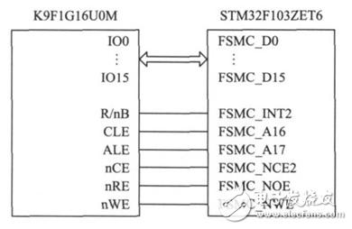
Figure 2 NANDFLASH and STM32F103ZET6 connection diagram
2.2, Ethernet interface circuit design
The use of an Ethernet interface instead of a traditional serial port speeds up data transfer and enables remote control. Since the STM32F103ZET6 does not have integrated Ethernet MAC and PHY functions, its FSMC supports extended Ethernet control chip. This system expands a DAVICOM DM9000A chip on the FSMC to extend the Ethernet of the STM32F103ZET6. The connection between the DM9000A and the STM32F103ZET6 is shown in Figure 3. Shown.
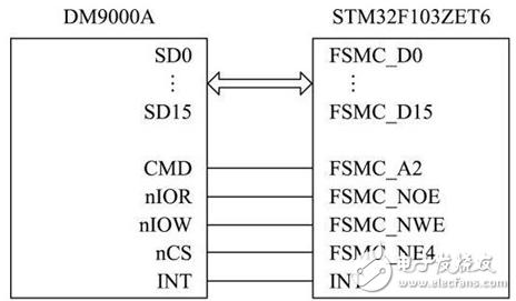
Figure 3 DM9000A and STM32F103ZET6 connection diagram
STM32F103ZET6 accesses DM9000A through FSMC. For STM32F103ZET6, DM9000A is a static memory peripheral. The DM9000A adopts 16-bit mode, and the data lines SD0~SD15 are directly connected to the lower 16 bits FSMC_D0~FSMC_D15 of the FMSC data line; the DM9000A chip select signal line nCS is connected to the FSMC chip select signal FSMC_NE4, so that the DM9000A port address is 0x6c000000; the DM9000A interrupt signal line INT can be directly connected to the IO port of STM32F103ZET6, activate the interrupt multiplexing function of the processor IO port in the program, and STM32 receives the network card data in interrupt mode.
2.3, scan drive circuit design
The scan drive circuit is an important part of the whole control system. In the system, it consists of an FPGA and a dual-body RAM. Its structure is shown in Figure 4. It mainly performs gray-scale data reading, generation and transmission of upper-screen data, and shifting. And the generation of the latch clock, the generation of the row selection signal, and the generation of the gradation control signal.
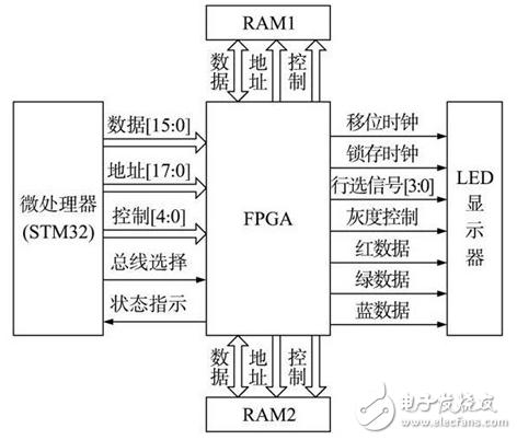
Figure 4 scan drive circuit structure
The simulation waveform of the scan drive output signal is shown in Figure 5, where en is the grayscale control signal used to control the display time and produce the grayscale effect; row_sel is the row select signal, which is used to determine which row is lit when displayed; sck is Shift clock, lck is the latch clock, ds_red, ds_blue, ds_green are the input of the upper red, blue and green data. During the simulation, the red, blue, and green display data are set to 01 interlace, all 1, and all 0. It can be seen that the data shift is correct under the action of the shift clock. After the shift is completed, lck becomes a high level, and the data is latched and outputted to the LED screen for display.

Figure 5 Simulation waveform of the output signal
3, system software design
The software of the whole system includes three parts: the upper computer application software, the microprocessor control software and the FPGA control software. The three parts work together to achieve control of the LED display.
3.1, PC application software
The upper computer application software is used for human-computer interaction, and is the interface of the control system to the user, requiring a friendly interface and simple operation. The software is written in Visual C++. The main functions completed include: editing of image text information, decoding of images, and sending data to the lower computer according to the communication protocol.
3.2, microprocessor control software
The microprocessor plays the role of core scheduling in the whole system. It controls the working state of each functional module of the system. The program includes the transplantation of TCP/IP protocol stack, DM9000A network card driver, etc. The main functions completed are: hardware initialization. Ethernet communication between the host computer and the lower computer, display mode algorithm design, etc.
3.3, FPGA control software
The FPGA control software was designed in the Quartus II environment and written in the hardware description language Verilog. The main function is to switch the memory according to the control of the microprocessor to realize the ping-pong operation; to complete the reconstruction of the image data, and convert the data into a coding series composed of 0 and 1 which can be directly used for LED scanning display and containing gray information. And according to the timing of the display driver chip, the code series is transmitted to the display on the display.
4, summary
This design uses a 32-bit embedded microprocessor STM32F103ZET6 and programmable logic device EP1C6Q240C8 to design a full-color LED display control system, and verified in the laboratory to achieve the color display of the LED display, Figure 6 (a) is an actual The image, Figure 6(b), shows the effect on the display.
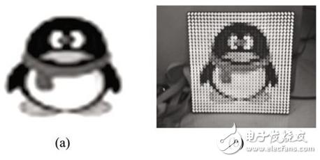
Figure 6 Grayscale display of the image
The experimental results show that the system runs stably and the display is clear and smooth. The system can meet the requirements of high processing speed of asynchronous full-color LED display, large-capacity data storage, support 256 gray-scale full-color image, animation display, and easily upgrade the system by changing the hardware logic inside the FPGA. The utility model has the advantages of simple structure and high reliability, and can replace the similar design products on the market, and has wide application prospects.
Instruction Manual
1. Features
Clock display, 10 sets of adjustable timed power control, randomized power control, manual switch and optional DST setup.
2. First time charging
This timer contains a rechargeable battery. It is normal that the new/old model runs out of battery if it wasn`t being charged for a long period of time. In this case, the screen will not turn on.
To charge : simply plug the timer to a power outlet. The charging time should take at least 15 minutes.
If the screen doesn`t light up or displays garbled characters, simply reboot the system by pressing the [RESET" button.
3. Set clock
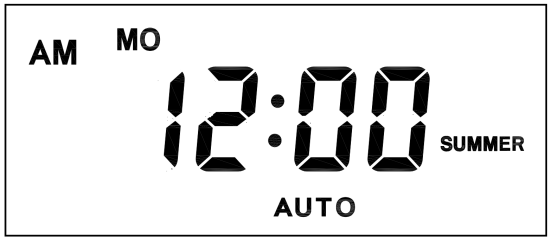
Hold [CLOCK" button and [WEEK" button to adjust week.
Hold [CLOCK" button and [HOUR" button to adjust hour.
Hold [CLOCK" button and [MINUTE" button to adjust minute.
Hold [CLOCK" button and [TIMER" button to select 12 hour/24 hour display.
Hold [CLOCK" button and [ON/AUTO/OFF" button to enable/disable DST (daylight-saving-time).
4. Set timer
Press [TIMER" button, select and set timer. Setting rotation : 1on, 1off, 2on, 2off, ...... , 10on, 10off.
Press [HOUR" button to set hour for timer.
Press [MIN" button to set minute for timer.
Press [WEEK" button to set weekday for timer. Multiple weekdays can be selected. ex: if selected [MO", the timer will only apply on every Monday; if selected [ MO, WE, FR", the timer will apply on every Monday, Wednesday and Friday.
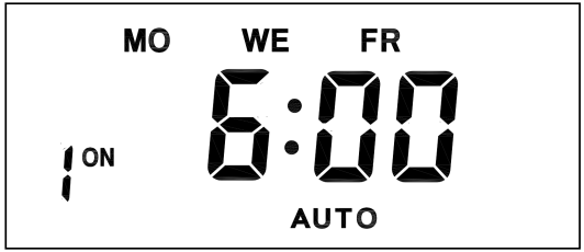
Press [RES/RCL" button to cancel the selected on or off timer. The screen will show "-- -- : -- --" , the timer is canceled.
Press [RES/RCL" button again to reactivate the timer.

When timers are set, press [CLOCK" to quit timer setting and return to clock.
5. Random function

Press [RANDOM" button to activate random function, press again to cancel function.
System only runs random function when [AUTO" is on.
Random function will automatically start the timer from 2 to 32 minutes after the setting.
ex : if timer 1on was set to 19:30 with the random function on, the timer will activate randomly between 19:33 to 20:03.
if timer 1off was set to 23:00 with the random function on, the timer will activate randomly between 23:02 to 23:32.
To avoid overlapping, make sure to leave a minimum of 31 minutes gap between different sets of timer.
6. Manual control
Displayed features:
ON : socket turns on.
OFF : socket turns off.
AUTO : socket turns on/off automatically via timer.
Manual ON setting
Press [ON/AUTO/OFF" button to switch from [AUTO" to [ON".
This mode allows socket of the device to power up. Power indicator will light up.
Manual OFF setting
Press [ON/AUTO/OFF" button to switch from [AUTO" to [OFF".
This mode turns socket of the device off. Power indicators will turn off.
7. Electrical parameters
Operating voltage : 230VAC
Battery : NiMh 1.2V
Power consumption : < 0.9W
Response time : 1 minute
Power output : 230VAC/16A/3680W
Q&A
Q: Why won`t my timer turn on?
A: It`s out of battery, you can charge the timer by plugging onto any power outlet. Charge the device for at least 15 minutes. Then press [RESET " button to reset the device.
Q: Can I set seconds of the timer?
A: No, the smallest time unit is minute.
Q: Does my timer keeps old settings without being plugged onto a power outlet?
A: Yes, the timer has an internal battery, it allows the timer to save settings without a power outlet.
Q: Is the battery rechargeable?
A: Yes, the battery is rechargeable. We recommend to charge it for 4 hours so the battery is fully charged.
Q: Does the timer needs internet connection?
A: The timer does not need internet.
Q: Does the screen have back light function?
A: It doesn`t support back light.
Digital Timer Socket, Timing Switch Socket, Electronic Timer Socket, Timer Socket
NINGBO COWELL ELECTRONICS & TECHNOLOGY CO., LTD , https://www.cowellsockets.com