The X1226 has a clock and calendar function, the clock relies on the hours, minutes and seconds registers to track, the calendar relies on the date, week, month and year registers to track, the calendar can be correctly displayed until 2099, and has an automatic leap year correction function. Has a powerful dual alarm function that can be set to any clock/calendar value with an accuracy of 1 second. Software can be used to set any of 1Hz, 4096Hz or 32768Hz frequency output.
The X1226 provides a backup power input pin, VBACK, which allows the device to use a battery or bulk capacitor for backup power. When using a capacitor, a silicon or Schottky diode is used to connect both ends of the Vcc and the charging capacitor. The charging capacitor is connected to the Vback pin. Do not use a diode to charge the battery (especially a Li-Ion battery). The condition for switching to battery power is Vcc=Vback-0.1V. During normal operation, the supply voltage Vcc must be higher than the battery voltage, otherwise the battery power will be gradually exhausted. The oscillator uses an external 32.768kH crystal, and the generated oscillation error can be corrected by software to adjust the values ​​of the digital trim register and the analog trim register, thus avoiding the influence of the external resistor and the dispersion of the capacitor on the accuracy. The 4Kb EEPROM can be used to store user data.
Circuit composition and working principleThe X1226 can interface with various types of microcontrollers or microprocessors. The interface is a serial I2C interface. The data bus SDA is a bidirectional pin for inputting or outputting data. The open-drain output of the device requires the addition of a 4.7- to 10-kΩ pull-up resistor during use. This article describes the 89C51 microcontroller and X1226 interface method, because the 89C51 microcontroller does not have a standard I2C interface, can only be simulated with software.
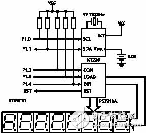
figure 1
In order to see the change of time more intuitively, 8-bit LED digital tube is used to display the year, month, day or hours, minutes and seconds. The PS7219A is used to drive the LED digital tube, and the digital tube selects the 0.5-inch common cathode red or green LED digital tube. Because the PS7219A device contains the IMP810 microcontroller monitoring device, the reset output is active high. Therefore, when the 51 system is used, there is no need to add a monitoring device. The reset output of the PS7219A can be used to reset the 51 single-chip microcomputer. The monitoring voltage is 4.63V. Hardware design schematic shown in Figure 1.
During the hardware power-on debugging process, the X1226 crystal oscillator must not be touched by hand. Otherwise, the oscillator may stop. To restore oscillator start-up, turn off the power (including the backup power supply) and then restart the power supply. In addition, it should be noted that, when measuring the oscillator, do not use the probe of the oscilloscope to measure the oscillation output of X2. Use the probe to measure the oscillation output of PHZ/IRQ to determine whether the oscillation and oscillation frequency are accurate. Add a 5.1kΩ pull-up resistor to the pin.
software designThe X1226 contains a real-time clock register (RTC), status register (SR), control register (CONTROL), alarm registers (Alarm0, Alarm1), and memory for the user to store data. Because the real-time clock registers and status registers require frequent write operations, the memory structure is a volatile SRAM structure. Other registers are EEPROM structures, and the number of write operations is usually more than 100,000 times. X1226 initialization program block diagram shown in Figure 2, the role of the subroutine YS4 delay 4μs.
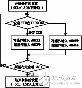
figure 2
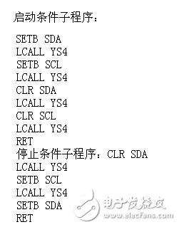
After X1226 initializes, the one-chip computer sets up and begins the condition to X1226, before writing CCR or EEPROM, the host must write 02H to the status register first, confirm the reply signal, write 06H after confirmation, confirm the reply signal again. The write operation is initiated after confirmation and the high place is sent first
Address, then send the lower address. Each X1226 will generate a response signal after receiving an address byte. After both address bytes are received, X1226 waits for 8 bits of data. After receiving the 8-bit data, X1226 generates another response, and then the microcontroller generates a stop condition to terminate the transfer.
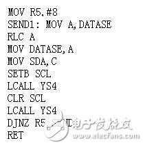
The X1226 has a continuous write function. Each time it receives a byte, it responds with a response and internally increments the address by one. When the counter reaches the end of the page, it automatically returns to the first address of the page. This means that the microcontroller can continuously write 64 bytes to the memory array from any position on a page, or write 8 bytes of data to the CCR. Write the X1226 data subroutine:
On power-up, the default value of the 16-bit address is 0000H. After the X1226 is initialized, the microcontroller sets the start conditions for the X1226. Before writing the CCR or EEPROM, the host must write 02H to the status register to confirm the response signal. After confirming that, write 06H and confirm the response signal. A write operation is initiated after the acknowledgement, first the upper address is sent, then the lower address is sent. Each X1226 will generate a response signal after receiving an address byte. The microcontroller sends another start condition, setting the R/W bit to 1, and then accepting 8-bit data. When the microcontroller terminates the read operation, the microcontroller can set the stop condition without waiting for the X1226's acknowledge signal. Read the X1226 data subroutine:
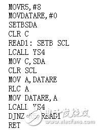
The X1226 integrates an oscillator compensation circuit. The user can fine-tune the oscillator frequency in software. This fine-tuning is usually applied to both cases. In one case, the oscillator is compensated for the frequency deviation caused by the initial accuracy of the device at a normal temperature of 25° C. The second case is to compensate for temperature-induced frequency drift. The X1226 has a digital trim register (DTR) and an analog trim register (ATR). Both registers are non-volatile registers. The digital trim register has a 3-bit digital trimming bit with an adjustment range of -30 to +30 & TImes; 10-6. The analog trim register has six analog trim bits with a regulation range of -37 to +116 & TImes; 10-6.
For compensation of temperature drift caused by changes in the external environment temperature, a compensation parameter table must be established in the memory according to the temperature coefficient of the crystal. The temperature coefficients of the crystals of different manufacturers are not the same and should be selected according to the product data sheet.
In order to be able to compensate for the temperature drift, a temperature sensor is required in the system, and it should be as close as possible to the X1226. This can truly reflect the temperature of the oscillator. The schematic diagram is shown in Figure 3. The one-chip computer first obtains the ambient temperature through the system temperature sensor, and obtains the corresponding compensation value in the compensation parameter table, then fills in the compensation data in the corresponding fine-tuning register, can realize the temperature drift compensation goal.

image 3
Because X1226 has a precise oscillator compensation function, it is very suitable for applications with large changes in ambient temperature, but also reduces the requirements on the crystal performance parameters
The following also introduces a program for readers:
;;;;;;;;;;;;;;;;;;;;;;;;;;;;;;;;;;;;;;;;;
;; AT89C2051 clock program;;
;;;;;;;;;;;;;;;;;;;;;;;;;;;;;;;;;;;;;;;;;
;
Timer T0, T1 overflow period is 50MS, T0 is used for counting seconds, T1 is used for flashing during adjustment.
P3.7 is the adjustment button, P1 port is the character output port, using common anode display tube.
;
;;;;;;;;;;;;;;;;;;;;;;;;;;;;;;;;;;;;;;;;;
;; interrupt entry program;;
;;;;;;;;;;;;;;;;;;;;;;;;;;;;;;;;;;;;;;;;;
;
ORG 0000H ; Program execution start address
LJMP START ; Jump to label START
ORG 0003H; External interrupt 0 interrupt program entry
RETI; External Interrupt 0 Interrupt Return
ORG 000BH Timer T0 interrupt program entry
LJMP INTT0 ; Jump to INTTO execution
ORG 0013H ; External interrupt 1 interrupt program entry
RETI; External Interrupt 1 Interrupt Return
ORG 001BH Timer T1 interrupt program entry
LJMP INTT1 ; skip to INTT1 execution
ORG 0023H ; Serial interrupt program entry address
RETI ; Serial Interrupt Program Return
;
;;;;;;;;;;;;;;;;;;;;;;;;;;;;;;;;;;;;;;;;
;; Main program;;
;;;;;;;;;;;;;;;;;;;;;;;;;;;;;;;;;;;;;;;;
;
START: MOV R0, #70H; Clear 70H-7AH Total 11 Memory Units
MOV R7, #0BH;
CLEARDISP: MOV @R0,#00H ;
INC R0 ;
DJNZ R7, CLEARDISP;
MOV 20H, #00H; Clear 20H (for signage)
MOV 7AH, #0AH ; Put "extinguishment" data
MOV TMOD, #11H ; Let T0 and T1 be 16-bit timers
MOV TL0, #0B0H ; 50MS timing initial value (for T0 timing)
MOV TH0, #3CH ;50MS initial value
MOV TL1, #0B0H ;50MS initial value (for T1 flash timing)
MOV TH1, #3CH; 50MS initial value
SETB EA; total interruption open
SETB ET0 ; Allow T0 interrupt
SETB TR0 ; Turn on T0 timer
MOV R4, #14H; 1 second timer initial value (50MS x 20)
START1: LCALL DISPLAY ; Call display subroutine
JNB P3.7, SETMM1 ; P3.7 is 0 when the transfer time adjustment process
SJMP START1 ; Jump to START1 when P3.7 is 1.
SETMM1: LJMP SETMM ; Go to time adjustment program SETMM
;
;;;;;;;;;;;;;;;;;;;;;;;;;;;;;;;;;;;;;;;;;
;; 1 second timer program;;
;;;;;;;;;;;;;;;;;;;;;;;;;;;;;;;;;;;;;;;;;
; T0 interrupt service routine
INTT0: PUSH ACC ; Accumulator Stack Protection
PUSH PSW ; Status Word Stack Protection
CLR ET0 ; Off T0 interrupt enable
CLR TR0 ; Turn off timer T0
MOV A, #0B7H ; Interrupt response time synchronization correction
ADD A, TL0 ; Lower 8-bit initial value correction
MOV TL0,A ; Reload initial value (low 8-bit correction value)
MOV A, #3CH ; High 8-bit initial value correction
ADDC A,TH0 ;
MOV TH0,A ;Reload initial value (high 8-bit correction value)
SETB TR0 ; Turn on timer T0
DJNZ R4, OUTT0 ; 20 interrupts did not exit the interrupt to exit
ADDSS: MOV R4, #14H; 20 interrupts to (1 second) initial value
MOV R0, #71H; Pointing to Second Timing Unit (71H-72H)
ACALL ADD1 ; call plus 1 program (plus 1 second operation)
MOV A, R3; second data into A (R3 is a 2-digit decimal combination)
CLR C ; Clearance Flag
CJNE A, #60H, ADDMM;
ADDMM: JC OUTT0 ; Exit if less than 60 seconds
ACALL CLR0 ; Clears the second timing unit greater than or equal to 60 seconds
MOV R0, #77H ;Pointing to the Timing Unit (76H-77H)
ACALL ADD1 ; Timekeeping unit plus 1 minute
MOV A, R3 ; Subdata into A
CLR C ; Clearance Flag
CJNE A, #60H, ADDHH;
ADDHH: JC OUTT0 ; Exit if less than 60 minutes
ACALL CLR0 ; Hours greater than or equal to 60 minutes
MOV R0, #79H ;Pointing Hours Timing Unit (78H-79H)
ACALL ADD1 ; hour time unit plus 1 hour
MOV A, R3; time data into A
CLR C ; Clearance Flag
CJNE A, #24H, HOUR;
HOUR: JC OUTT0 ; Exit less than 24 hours
ACALL CLR0 ; Hours greater than or equal to 24 hours
OUTT0: MOV 72H, 76H; Moves the data of timing and timing units when the interrupt is exited
MOV 73H,77H ;Input corresponding display unit
MOV 74H, 78H;
MOV 75H, 79H;
POP PSW ; Resume Status Word (Push)
POP ACC ; Recover Accumulator
SETB ET0 ; Open T0 interrupt
RETI; interrupt return
;
;;;;;;;;;;;;;;;;;;;;;;;;;;;;;;;;;;;;;;;;;
;; flashing time adjustment program;;
;;;;;;;;;;;;;;;;;;;;;;;;;;;;;;;;;;;;;;;;;
; T1 interrupt service routine, used to adjust unit flash indication when time is adjusted
INTT1: PUSH ACC; Interrupted Site Protection
PUSH PSW;
MOV TL1, #0B0H ; Install timer T1 timing initial value
MOV TH1, #3CH;
DJNZ R2, INTT1OUT ; 0.3 seconds did not exit the interrupt (50MS interrupt 6 times)
MOV R2, #06H ; reload 0.3 seconds timer initial value
CPL 02H; 0.3 second timer to reverse the blinking flag
JB 02H, FLASH1 ; The 02H bit is 1 when the display unit "extinguishes"
MOV 72H, 76H ; Normal display when 02H bit is 0
MOV 73H, 77H;
MOV 74H, 78H;
MOV 75H, 79H;
INTT1OUT:
POP PSW;Restoration
POP ACC
RETI; Interrupted Exit
FLASH1: JB 01H, FLASH2 ; When 01H bit is set to 1, the hour turns off the control
MOV 72H, 7AH ; 01H bit is 0, the "extinguishment" data into points
MOV 73H, 7AH; display unit (72H-73H), no subdata will be displayed
MOV 74H, 78H;
MOV 75H, 79H;
AJMP INTT1OUT ; transfer interrupt exit
FLASH2: MOV 72H, 76H; 01H bit is 1, when the "extinguishing" data is put into the hour
MOV 73H, 77H; Display Unit (74H-75H), hour data will not be displayed
MOV 74H, 7AH;
MOV 75H, 7AH;
AJMP INTT1OUT ; transfer interrupt exit
;
;;;;;;;;;;;;;;;;;;;;;;;;;;;;;;;;;;;;;;;;;
;; Add 1 subroutine;;
;;;;;;;;;;;;;;;;;;;;;;;;;;;;;;;;;;;;;;;;;
;
ADD1: MOV A, @R0 ; Take current timing unit data to A
DEC R0 ; points to the previous address
SWAP A; A data exchange between the upper and lower four digits
ORL A, @R0 ; the data in the previous address is put into the lower four bits of A
ADD A, #01H ; A plus 1 operation
DA A; Decimal adjustment
MOV R3,A ; Move into R3 register
ANL A, #0FH ; High-order four bits become 0
MOV @R0,A ;Replace the previous address unit
MOV A, R3 ; Retrieve temporary data in R3
INC R0 ; points to the current address unit
SWAP A; A data exchange between the upper and lower four digits
ANL A, #0FH ; High-order four bits become 0
MOV @R0,A ; Data is placed in the address cell
RET; Subroutine return
;
;;;;;;;;;;;;;;;;;;;;;;;;;;;;;;;;;;;;;;;;;
;; Clear program;;
;;;;;;;;;;;;;;;;;;;;;;;;;;;;;;;;;;;;;;;;;
; Use the timing unit to zero
CLR0: CLR A ; Clear Accumulator
MOV @R0,A ; Clear Current Address Unit
DEC R0 ; points to the previous address
MOV @R0,A ; Clear the previous address unit
RET; Subroutine return
;
;;;;;;;;;;;;;;;;;;;;;;;;;;;;;;;;;;;;;;;;;
;; Clock adjustment program;;
;;;;;;;;;;;;;;;;;;;;;;;;;;;;;;;;;;;;;;;;;
; Enter this program when the key is pressed
SETMM: cLR ET0 ; Off Timer T0 Interrupt
CLR TR0 ; Turn off timer T0
LCALL DL1S ;call one second delay program
JB P3.7, CLOSEDIS ; The key press time is less than 1 second, turn off the display (power saving)
MOV R2, #06H ; Enter the time adjustment status, and give the blinking timer initial value
SETB ET1 ; Allow T1 interrupt
SETB TR1 ; Turn on timer T1
SET2: JNB P3.7, SET1; P3.7 is 0 (key not released), waiting
SETB 00H ;Key release, minute adjustment flashing flag set
SET4: JB P3.7, SET3 ; wait key pressed
LCALL DL05S; A key press, delay 0.5 seconds
JNB P3.7,SETHH; Pressing time is greater than 0.5 seconds
MOV R0, #77H; Press time less than 0.5 seconds plus 1 minute operation
LCALL ADD1 ; call plus 1 subroutine
MOV A, R3 ; Take adjustment unit data
CLR C ; Clearance Flag
CJNE A, #60H, HHH; Adjustment Unit Data Compared to 60
HHH: JC SET4; Adjust cell data less than 60 revolutions SET4 loop
LCALL CLR0 ; Cleared when the adjustment unit data is greater than or equal to 60
CLR C ; Clearance Flag
AJMP SET4 ; Jump to SET4 loop
CLOSEDIS: SETB ET0; power saving (LED not shown) status. Open T0 interrupt
SETB TR0 ; Turn on T0 timer (clock on)
CLOSE: JB P3.7, CLOSE ; No button pressed, wait.
LCALL DISPLAY; Press the key to adjust the subroutine delay shading
JB P3.7, CLOSE ; is a disturbance return CLOSE wait
WAITH: JNB P3.7, WAITH; waiting for key release
LJMP START1 ; Return to main program (LED data display is on)
SETHH: CLR 00H; minute flash flag cleared (into the hourly state)
SETHH1: JNB P3.7, SET5; wait for key release
SETB 01H; Hour adjustment flag set to 1
SET6: JB P3.7, SET7; waiting for key presses
LCALL DL05S; With key press delay 0.5 seconds
JNB P3.7, SETOUT; Press time is greater than 0.5 seconds to exit time adjustment
MOV R0, #79H; Press time less than 0.5 seconds plus 1 hour operation
LCALL ADD1 ; Add 1 subroutine
MOV A, R3 ;
CLR C ;
CJNE A, #24H, HOUU; Comparison of timing unit data with 24
HOUU: JC SET6 ; Less than 24 turns to SET6 loop
LCALL CLR0 ; Cleared to 0 when greater than or equal to 24
AJMP SET6 ; Jump to SET6 loop
SETOUT: JNB P3.7, SETOUT1 ; Exit the program when adjusted. Wait for key release
LCALL DISPLAY ; Delay Shake
JNB P3.7, SETOUT ; is dithered, returns to SETOUT and waits again
CLR 01H; Clearance Hours Sign
CLR 00H; Clearance Mark
CLR 02H; Clear blinking mark
CLR TR1 ; Turn off timer T1
CLR ET1 ; Off Timer T1 Interrupt
SETB TR0 ; Turn on timer T0
SETB ET0 ; Open timer T0 interrupt (time start)
LJMP START1 ; Skip back to main program
SET1: LCALL DISPLAY ; Call the display program when the key is released waiting (adjustment)
AJMP SET2 ; No clock display when the key is pressed
SET3: LCALL DISPLAY ; Clock display when waiting for adjustment button
AJMP SET4
SET5: LCALL DISPLAY ; The display program is called when the key is released waiting (hourly adjustment)
AJMP SETHH1 ; No clock display when the key is pressed
SET7: LCALL DISPLAY ; Clock display when waiting for key adjustment
AJMP SET6
SETOUT1: LCALL DISPLAY ; Key release waits when exiting clock adjustment
AJMP SETOUT ; No clock is displayed when the key is pressed
;
;;;;;;;;;;;;;;;;;;;;;;;;;;;;;;;;;;;;;;;;;
;; Display program;;
;;;;;;;;;;;;;;;;;;;;;;;;;;;;;;;;;;;;;;;;;
Display data in the 70H-75H unit, using six LED digital LED display, P1 output section code data, P3 mouthpiece
Scan control, each LED digital tube light 1MS time and then bit by bit cycle.
DISPLAY: MOV R1, #70H ; Point to display data first address
MOV R5, #0FEH ; Scan Control Word Initial Value
PLAY: MOV A,R5 ;Scanning words into A
MOV P3, A ; output from port P3
MOV A, @R1 ; Take display data to A
MOV DPTR, #TAB; fetch segment table address
MOVC A, @A+DPTR; Check Display Data Corresponding to Segment Codes
MOV P1, A ; Segment code inserted into port P1
LCALL DL1MS ; Display 1MS
INC R1 ; points to the next address
MOV A, R5 ; Scan control word into A
JNB ACC.5, ENDOUT ; ACC.5=0 shows once
RL A ; The data loops left in A
MOV R5,A ;Return to R5
AJMP PLAY ; Jump back to PLAY loop
ENDOUT: SETB P3.5 ; The end of a display, P3 reset
MOV P1, #0FFH ; Port 1 reset
RET; Subroutine return
TAB: DB 0C0H, 0F9H, 0A4H, 0B0H, 99H, 92H, 82H, 0F8H, 80H, 90H, 0FFH
;Yangyang section code table "0", "1", "2", "3", "4", "5", "6", "7", "8", "9", "unlit"
;
;;;;;;;;;;;;;;;;;;;;;;;;;;;;;;;;;;;;;;;;;
;; Delay program;;
;;;;;;;;;;;;;;;;;;;;;;;;;;;;;;;;;;;;;;;;;
;
1MS delay program, LED display program
DL1MS: MOV R6, #14H
DL1: MOV R7, #19H
DL2: DJNZ R7, DL2
DJNZ R6, DL1
RET
20MS time-delay program, call display subroutine to improve LED display flicker
DS20MS: ACALL DISPLAY
ACALL DISPLAY
ACALL DISPLAY
RET
; Delayed program, used as a key to determine the length of time
DL1S: LCALL DL05S
LCALL DL05S
RET
DL05S: MOV R3, #20H; 8 milliseconds * 32 = 0.196 seconds
DL05S1: LCALL DISPLAY
DJNZ R3, DL05S1
RET
;
END ; End of program
Pouch Cell,Lithium-Ion Pouch Cell,Lifepo4 Pouch Cell,Lithium Battery Pouch
JIANGMEN RONDA LITHIUM BATTERY CO., LTD. , https://www.ronda-battery.com