With the popularity of fingerprint recognition on smartphones, fingerprint recognition technology has been applied in more and more occasions. In addition to mobile applications, it has also become popular in embedded scenarios such as mobile payments, access control systems, and smart homes. In the system implementation, the smart phone itself has powerful computing power and rich memory resources. It is not difficult to realize fingerprint recognition. However, in embedded systems, especially in MCU-based applications, its computing power and memory resources are limited. This paper introduces a fingerprint recognition scheme and design points based on single-chip microcomputer system.

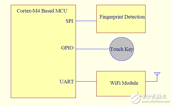
As shown in the above figure, this is a system block diagram of the WiFi fingerprint recognition front end. The application scenario is: when the finger presses the fingerprint recognition module, the fingerprint data is collected and transmitted to the single-chip microcomputer, and the single-chip computer processes the fingerprint data through the recognition algorithm, and then processes the The result is wirelessly transmitted to the cloud to participate in the identity identification service through the WiFi module.
In the specific implementation, since the fingerprint recognition algorithm involves more floating-point operations, and needs to temporarily store the original data and the intermediate operation data of the fingerprint lattice, there is a hard requirement for the computing power and the storage space, and the current mainstream single-chip architecture The Cortex-M4 architecture integrates the FPU floating-point processing unit, and its floating-point arithmetic capability can meet the requirements at a frequency of 100 MHz. After the fingerprint identification algorithm code is compiled, it takes up hundreds of kilobytes of code space. Considering the WiFi network connection and the application layer code, it is better to use about 1MB of Flash code space as a whole, and the data storage requirement is 512KB of SRAM space. When the system works, it needs powerful computing power in the fingerprint identification process, and when there is no fingerprint pressing, it needs to run in the low power state to meet the power consumption requirements of the embedded system.
In our solution, the MCU with XIP features is selected, and the code is stored in the external SPI Flash and can be executed in the system, which greatly expands the code storage space. The code in the external SPI Flash is slightly slower in execution because it requires an internal Cache cache. For the core code of the recognition algorithm, it can be copied to the SRAM during the Boot phase to improve the running speed. XIP + SRAM's code space allocation scheme combines performance and cost, and is a highlight of this design.
The fingerprint identification chip is the core component of the system implementation. Currently, the mainstream technical indicators require the fingerprint recognition chip to be based on capacitive technology, support Live Detection (Live Finger DetecTIon), push type, and use glass cover to achieve 360-degree touch in any direction. , able to support sliding navigation. The living body detection technology has the feature of preventing false fingerprint cracking, and integrates heart rate detection function, which is convenient for the user to view the heart rate value in real time. The integration of the sensor facilitates the design of the whole machine manufacturer and the integration of the whole machine, making it convenient to be applied to the embedded single chip system.
The data interface between the fingerprint identification chip and the host requires a transmission rate of 5 Mbps or more in the process of fingerprint data acquisition, and the data throughput below 5 Mbps will affect the user experience. Low-speed interfaces such as UART and I2C cannot meet the requirements in terms of throughput. The SPI interface is simple and the transmission rate can meet the requirements. It is the most suitable communication interface.
The fingerprint identification chip periodically detects whether there is a finger touch in the Pixel sensor area. When detecting that the sensor has a finger touch, the living body detection data is immediately collected. After the data acquisition is completed, the host is notified by the interrupt, and the MCU reads the living body detection data. Fingerprint scanning is performed, and after the fingerprint scanning starts, the host is notified by interrupt to read the data. The scanning of the fingerprint data and the reading of the host data are performed simultaneously.
The MCU receives the Pixel raw data transmitted by the fingerprint chip, and then transmits it to the cloud through the WiFi module after being processed by the recognition algorithm. Due to the limitations of the MCU's own resources, the WiFi module itself needs to integrate the WiFi driver, TCP/IP protocol stack, and can run the application layer code as a relatively independent unit, which greatly reduces the burden on the MCU host. The WiFi module exchanges data with the MCU through the serial port. A WiFi IoT module based on the Qualcomm QCA4004 is recommended.

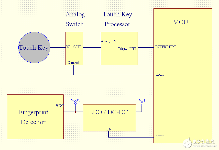
Low power consumption and anti-jamming are also a key point of the system design. The fingerprint recognition module periodically scans the sensor without finger pressing. Although the power consumption is lower than the data transmission period, in order to adapt to the battery power supply, it is hoped that there is no button. During the touch, the power of the fingerprint recognition module can be turned off. For this reason, the touch button is added as shown in the above figure, and when the finger is detected, the power of the fingerprint recognition chip is turned on, and the fingerprint scanning data is collected, when there is no finger touch for a long time. Turn off the power of the fingerprint scanning module to reduce power consumption. In addition, in order to prevent the influence of the touch button on the fingerprint recognition sensor during data acquisition, an analog switch is added after the touch button is pressed, and the MCU outputs a control signal to isolate the analog signal of the touch button before the start of the acquisition.
It is used for continuous level measurement. The signal transmitted by its sensor is collected by the receiving system after being reflected by the target, and the distance of the target is determined by measuring the reflection running time. Then the level distance is converted into an output signal and output as a measured value.
The liquid level radar is applicable to the continuous non-contact liquid level measurement of liquid cargo tanks and overflow tanks of oil tankers and chemical carriers. It is also applicable to the liquid level monitoring of other oil tanks, towers, tank equipment and oil production platforms. Its measurement results are not affected by medium replacement, temperature change and gas or steam coverage.
Radar Level Gauge Sensor,Level Gauge Sensor,Level Sensor Durable,Durable Radar Level Gauge Sensor
Taizhou Jiabo Instrument Technology Co., Ltd. , https://www.jbcbyq.com