As power densities continue to increase, soft switching topologies such as half-bridges (such as HID half-bridges or LLCs) and full-bridges (such as ZVS full-bridges) are the ideal solution. By improving the dynamic performance of di/dt and dv/dt on power devices, these topologies can reduce system switching losses and improve reliability. This situation mainly occurs under light load conditions. It has been proven that a superjunction device such as CoolMOS can overcome this problem by optimizing the charge carrier removal function of the reverse recovery process and eliminating the latching problem of the internal parasitic NPN bipolar transistor. By increasing the bonding rate of the injected carriers, the reverse recovery charge can be greatly reduced, and the enhanced bonding ratio can reduce the reverse recovery peak current during the turn-off process, and the reverse recovery charge can be greatly reduced to approximately tenths. one. The shape of the reverse recovery waveform and the design of the printed circuit board are especially important for optimizing the body diode (Figure 1) performance for hard switching applications. The new generation of CoolMOS 650V CFD2 improves body diode reverse recovery performance and leaves a greater margin of safety for breakdown voltage.
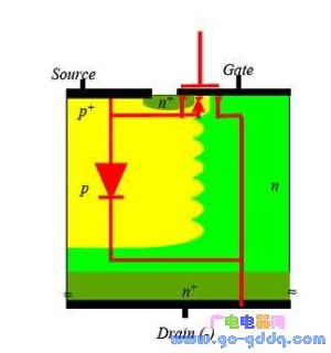
Figure 1 is a cross-sectional view of a CoolMOS high voltage power MOSFET and its internal body diode.
Reverse recovery behavior
The reverse recovery characteristics of the new generation CoolMOS 650V CFD are shown in Figure 2. Compared to standard devices, the new generation of CoolMOS 650V CFD devices have a very low reverse recovery charge Qrr, a very short reverse recovery time trr and a very small reverse recovery current maximum Irrm.
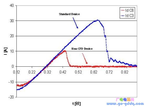
Fig. 2 is a reverse recovery waveform measured under conditions of di/dt = 100 A/μs, 25 ° C, and Vr = 400 V. Compared to standard devices, next-generation CFD devices have extremely low Qrr, trr, and Irrm.
At the same time, although the Qrr, trr, and Irrm are greatly reduced, the waveform of this new device still shows soft characteristics. This feature is ideal for hard commutation and is designed to avoid voltage overshoot and ensure reliable operation of the device.
Converter durability
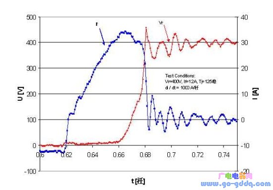
Figure 3. Reverse recovery waveform of the new generation CoolMOS 650V CFD2 device. These devices are not damaged even when the tester reaches maximum power.
The reverse recovery measurements of Figure 3 (under di/dt "2000A/μs) show the commutation durability of the CoolMOS(tm) 650V CFD2 device.
Under these conditions, no device was damaged. These waveforms still show soft characteristics relative to the highly fluctuating waveforms of other superjunction devices. Obviously, this is a big advantage for designers. Designers can maximize performance by optimizing their application without worrying about device damage during hard commutation of the body diode.
Qrr and trr and temperature
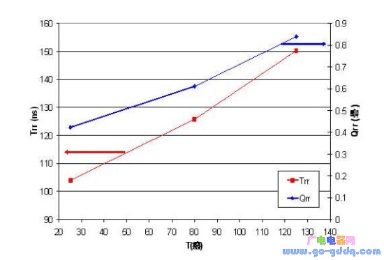
Figure 4. Qrr and Trr for a 310mΩ 650V CFD device versus temperature.
For designers, understanding Qrr and trr is critical to temperature. The Qrr and trr values ​​increase with increasing temperature because the carriers in the device increase at high temperatures. Figure 4 shows this relationship between Qrr and trr values ​​and temperature for a 310mΩ 650V CFD2 device. It can be seen from the graph that Qrr and trr are linear with temperature.
Relationship between Qrr and Trr and on-state resistance
Another important aspect to note is the relationship between Qrr and trr and the on-state resistance of the device, as shown in Figure 5 and Figure 6. Figures 5 and 6 compare a new generation of C6-based 650V CFD2 devices with Infineon's previous C3-based 600V CFD.
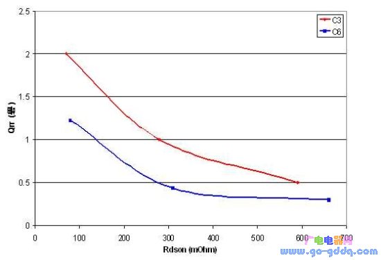
Figure 5 Qrr vs. on-state resistance, measured at 25 °C. Compare 80 mΩ, 310 mΩ, and 660mΩ 650V CFD2 devices to the previous generation C3 technology based 600V CFD.
Clearly, the new 650V CFD2 device achieves a better balance between dynamic characteristics (Qrr, trr) and lowest on-state resistance than previous generation technology.
An electrical appliance used to protect electrical equipment from high transient overvoltage hazards and to limit the duration of continuous flow.This term includes any external clearance necessary for the normal functioning of the appliance during operation and installation, whether or not it is a unit as a whole.
Surge protector, also known as lightning arrester, is an electronic device that provides safety protection for all kinds of electronic equipment, instruments and communication lines.When the electric circuit or communication lines or for outside disturbance suddenly produce peak current in voltage, surge protector in a very short time conduction tap, to avoid surge damage to other devices in the circuits.[1]
Surge protector, suitable for ac 50/60 hz, rated voltage 220 v to 380 v power supply system, the indirect lightning and thunder and lightning directly affect transient over voltage surge protection, or other applicable to the family home, the third industry and the surge protection industry requirements.
Surge Protector,Surge Voltage Protector,Eco-Friendly Surge Protector,Lightning Protection Surge Protector
YANGZHOU POSITIONING TECH CO., LTD. , https://www.pst-thyristor.com