The LM5117 is a synchronous buck controller for buck regulator applications with high voltage or various input supplies. The control method is based on current mode control using a simulated current ramp. Current mode control features inherent input voltage feedforward, cycle-by-cycle current limiting, and simplified loop compensation. Using analog control ramps reduces the sensitivity of the pulse width modulation circuitry to noise, helping to achieve reliable control of the extremely small duty cycle necessary for high input voltage applications.
The operating frequency of the LM5117 can be set from 50kHz to 750kHz. The LM5117 utilizes adaptive dead time control to drive external high-side and low-side NMOS power switches. User-selectable diode emulation mode enables non-continuous mode operation for improved efficiency under light load conditions. The high voltage bias regulator can further increase efficiency with an external bias supply. The LM5117's unique analog telemetry feature provides average output current information. Other features include thermal shutdown, frequency synchronization, hiccup mode current limit, and adjustable input undervoltage lockout. Today, I will talk about the buck circuit of the LM5117.
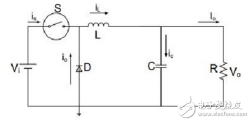
The BUCK circuit is one of the basic DC-DC circuits. The driving voltage is generally PWM (PulsewidthmodulaTIon pulse width modulation) signal, the signal period is Ts, the signal frequency is f=1/Ts, the on time is Ton, the off time For Toff, the period Ts = Ton + Toff, and the duty ratio Dy = Ton / Ts.

UVLO: From VIN to AGND, an external UVLO setpoint divider, RUV2, can be used to set the regulator's minimum input operating voltage. The divider must be designed when the input voltage is within the desired operating range. The UVLO pin can be clamped with a Zener diode. The UVLO hysteresis is accomplished by an internal 20A sink current that turns the impedance of the divider into the UVLO setpoint on or off. When the voltage at the UVLO pin exceeds the 1.25V threshold, the sink current is enabled, rapidly increasing the voltage at the UVLO pin. When the UVLO pin voltage drops below the 1.25V threshold, the sink current is disabled, causing the voltage on the UVLO pin to drop rapidly. Connecting the CFT capacitor in parallel with RUV1 helps minimize switching noise injected into the UVLO pin.

DEMB pin: In diode emulation mode, after detecting a reverse current flow (current flowing from output to ground through the low-side NMOS), the low-side NMOS is latched off during the rest of the PWM cycle. This pin is floating and the 50KΩ pull-down resistor inside the LM5117 keeps the DEMB pin low and enables diode emulation.
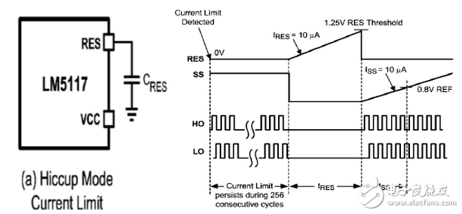
RES pin, SS pin: In order to further protect the regulator under long-term current limiting conditions, the LM5117 provides hiccup mode current limit. The internal hiccup mode fault timer counts the PWM clock period during which the cycle-by-cycle current limit occurs. When the discontinuous mode fault timer detects a current limit of 256 consecutive cycles, the internal restart timer forces the controller into a low-power standby mode and begins to sink 10uA of current into the RES pin capacitor CRES. In this standby mode, the HO and LO outputs are disabled and the soft-start capacitor SSC is discharged. CRES is connected from the RES pin to AGND to determine the time (tRES) to remain in standby before the LM5117 automatically restarts. When the RES pin voltage exceeds the 1.25VRES threshold, the RES capacitor is discharged and begins a soft-start sequence.

RT pin: The LM5117 switching frequency is set by an external resistor connected between the RT pin and the AGND pin. This resistor should be placed very close to the device and connected directly to the RT and AGND pins.
AGND: Analog ground. Internal 0.8V voltage reference circuit and analog circuit loop.
VCCDIS pin: VCCDIS has an internal 500KΩ pull-down resistor that enables the VCC regulator when this pin is floating.
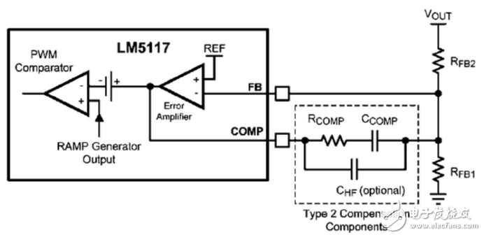
FB, COMP: The voltage divider signal (RFB1, RFB2) derived from the FB pin output sets the output voltage level. The internal high gain error amplifier produces an error signal proportional to the difference between the FB pin voltage and the internal high precision 0.8V reference. The output of the error amplifier connected to the COMP pin allows the user to implement Type II loop compensation components, namely RCOMP, CCOMP and optional CHF.

CM: It provides the average value of the detected inductor current. The monitor is connected directly between CM and AGND. When this pin is not used, the CM should be floating.
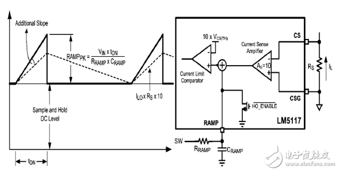
RAMP: External resistors and capacitors connected between the SW pin, the RAMP pin, and the AGND pin are used to set the PWM ramp slope. Select a suitable component value to generate a RAMP ramp signal.
CS, CSG: Pulse Width Modulator ramp signals for traditional current mode control are typically derived directly from the high side switch current. This switching current corresponds to the positive slope portion of the inductor current. The PWM ramp using this signal simplifies the control loop transfer function to a pole response while achieving inherent input voltage feedforward compensation. The disadvantage of using the high-side switch current signal for PWM control is that the leading edge spike is large because the parasitic effects of the circuit must be filtered or blanked. With a high-side current-sense circuit, the minimum achievable pulse width can be limited by filtering, blanking time, and propagation delay. In applications where the input voltage may be higher than the output voltage, controlling the small pulse width and duty cycle is necessary for voltage regulation. The LM5117 uses a unique ramp generator that does not actually measure the high-side switch current, but instead reconstructs this signal. Characterizing or simulating the inductor current provides a ramp signal to the PWM comparator that has no leading edge spikes and no measurement or filtering delays while maintaining the benefits of traditional peak current mode control. The current reconstruction consists of two parts: the sample and hold DC level and the simulated inductor current ramp, as shown in Figure 8. The sample and hold DC levels are derived from measuring the circulating current flowing through the current sense resistor. The voltage across the sense resistor can only be sampled and held before the next conduction time interval of the high side switch begins. The current sense amplifier has a gain of 10, the sample and hold circuit provides the DC level of the reconstructed current signal, and the positive slope inductor current ramp is simulated by a RAMPC connected between RAMP and AGND, and a RAMPR connected between SW and RAMP. The RAMPR should not be tied directly to VIN because at high input voltages, the voltage may exceed the absolute maximum voltage rating of the RAMP pin. During the off time, the CRAMP is discharged through an internal switching transistor and must be fully discharged during the minimum off time.

PGND: Power supply ground return pin for the low-side NMOS gate driver. Connect directly to the low side of the current sense resistor.
LO, HO: The LM5117 contains several high current NMOS drivers and an associated high side level converter to drive the external high side NMOS device. This high side gate driver works in conjunction with an external diode DHB and a bootstrap capacitor. The bootstrap capacitor is connected between the HB and SW pins with a short trace. During the off-time of the high-side NMOS driver, the SW pin voltage is approximately 0V, and CHB is charged from VCC via DHB. When operating at a high PWM duty cycle, the high-side NMOS device is forced to turn off for 320ns per cycle to ensure that the CHB is charged. The CSD18532KCSMOS FET is used in this design to reduce power consumption. LO and HO are respectively connected to the gate of the MOS transistor.
SW: Switch node of the buck regulator. The source of the high-side NMOS transistor and the drain of the low-side NMOS are connected to the bootstrap capacitor through a short, low-inductance path.
HB: High side driver power supply for bootstrap gate drive. Connect to the cathode and bootstrap capacitor of the external bootstrap diode. The bootstrap capacitor provides current for the high-side NMOS gate charge and should be placed as close as possible to the controller.
VIN: VCC regulator supply voltage input source.
Watch Screen Protector features a stretchable and retractable TPU Screen Protector that resists air bubbles and fingerprints on your device's screen and provides maximum protection for your device from scratches. The Hydrogel Film repairs screen scratches on its own and is ideal for curved curved screens.
Full Coverage: The soft material matches the edges of the watch screen well. Full coverage provides better protection and looks very discreet.
Oleophobic and waterproof: The oleophobic waterproof transparent layer can prevent the residue of sweat and grease, resist fingerprints, and keep the phone screen as new as ever.
Sensitive touch: only 0.14mm thick ultra-thin protective layer will not interfere with touch screen commands, your touch screen can still operate 100% normally.
If you want to know more information about Smart Watch Screen Protector products, please click the product details to view the parameters, models, pictures, prices and other information of Watch Screen Protector products.
Whether you are a group or an individual, we will do our best to provide you with accurate and comprehensive information about Watch Hydrogel Screen Protectors!
Watch Screen Protector, Watch Hydrogel Screen Protector,Smart Watch Screen Protector,Watch Protective Film,Apple Watch Screen Protector,Watch Screen Protector Cover
Shenzhen Jianjiantong Technology Co., Ltd. , https://www.jjthydrogelprotector.com